Avalanche photodiode

a photodiode and avalanche technology, applied in the field of avalanche photodiodes, can solve the problems of sacrificing sensitivity characteristics, noise characteristics and high-speed response characteristics, and deterioration of noise characteristics, so as to reduce working voltage, reduce noise characteristics, and reduce the effect of sensitivity

Inactive Publication Date: 2007-03-06
MITSUBISHI ELECTRIC CORP
View PDF3 Cites 18 Cited by
  • Summary
  • Abstract
  • Description
  • Claims
  • Application Information

AI Technical Summary

Benefits of technology

[0016]In view of the above situation, it is an object of the present invention to provide an avalanche photodiode which can be improved in low-noise characteristics and high-speed response characteristics and can provide high sensitivity.
[0018]In the present invention, impurities are added in a high concentration to a part of the light-absorbing layer to form a non-depletion region (a multiplication suppressing layer is inserted), whereby an avalanche photodiode can be attained which can be reduced in working voltage, has high sensitivity and low-noise characteristics and can attain high-speed response under low voltage.

Problems solved by technology

If the absorbing layer is made thick to better sensitivity, this gives rise to the problem that carriers multiplied in the absorbing layer are increased, resulting in deteriorations in noise characteristics and high-speed response characteristics.
Also, the absorbing layer must be made thin to improve low-noise characteristics and high-speed response characteristics, giving rise to the problem that sensitivity characteristics are sacrificed.

Method used


Image

  • Avalanche photodiode
  • Avalanche photodiode
  • Avalanche photodiode

Examples


embodiment 1

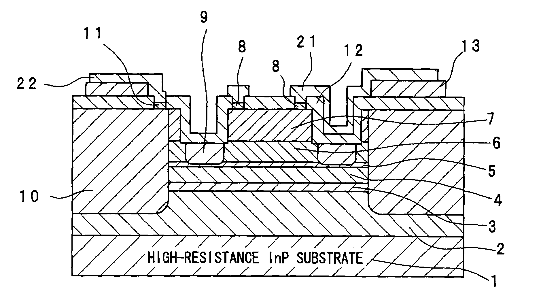
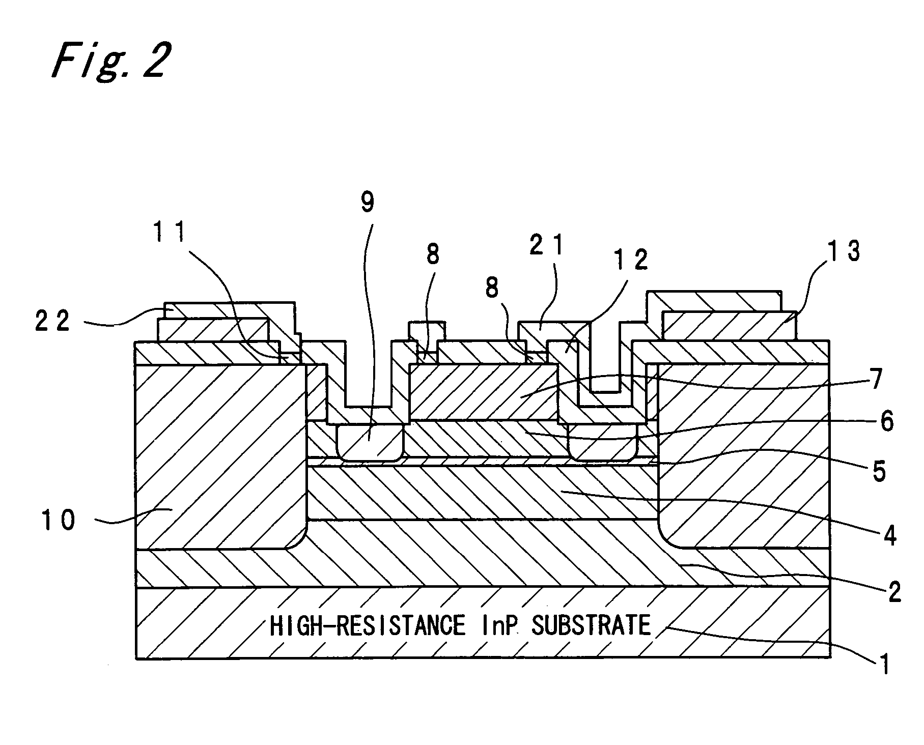
[0029]First, a specific structure of an avalanche photodiode in an embodiment 1 will be clarified by way of brief explanations of a process of producing the avalanche photodiode of the embodiment 1 according to the present invention.

[0030]The avalanche photodiode of the embodiment 1 is a plane light-receiving type separated absorption and multiplication avalanche photodiode (SAM-APD (Separated absorption and Multiplication-Avalanche Photo Diode)).

[0031]First, a p-type InP buffer layer 2 (Be: 5×1018 cm−3), a p-type InGaAs multiplication suppressing layer 3 (Be: 5×1017 cm−3), an i-type InGaAs light-absorbing layer 4, a p-type InP field limiting layer 5 (Be: 4.5×1017 cm−3), an i-type AlInAs multiplication layer 6, an i-type InP etching stopper layer (not shown), an n-type AlInAs cap layer 7 (Si: 5×1018 cm−3) and an n-type InGaAs contact layer 8 (Si: 5×1018 cm−3) are formed one by one by epitaxial growth. As a crystal growth method, a solid source or gas source MBE method, metalorganic ...

embodiment 2

[0064]FIG. 9 is a sectional view showing the elemental structure of an avalanche photodiode having a multiplication layer comprising i-type InP.

[0065]A process of producing the avalanche photodiode of the embodiment 2 will be briefly explained to clarify the structure of the avalanche photodiode of the embodiment 2.

[0066]In this method, first an n-type InGaAs multiplication suppressing layer 103 (Si: 1×1018 cm−3), an i-type InGaAs light-absorbing layer 104, an i-type InGaAsP layer 105, an i-type InP multiplication layer 106 and an i-type InGaAs contact layer 107 are respectively formed one by one on an n-type InP substrate 101 by epitaxial growth (impurities to be added to the crystal and the concentration of the impurities are shown in the above parenthesis). As the crystal growth method, solid source or gas source MBE, metalorganic chemical vapor deposition (MOCVD) method or the like is preferably used.

[0067]Next, the cyclic groove region is implanted with Be ions, followed by hea...

embodiment 3

[0075]In the embodiments 1 and 2, the structure in which light is incident from the upper surface of the element is described by way of explaining the process of producing the element. A semiconductor light-receiving element generically called a waveguide type avalanche photodiode in which light is incident from the element side (cleavage plane side) as shown in FIG. 10 can be expected to be improved in the ratio of ionization rates by inserting the InGaAs multiplication suppressing layer 203.

[0076]The avalanche photodiode of the embodiment 3 is produced in the following manner.

[0077]First, a p-type InGaAs conductive layer 201, a p-type InP layer 202, a p-type InGaAsP light-confining layer 211, a p-type InGaAs multiplication suppressing layer 203, an i-type InGaAs light-absorbing layer 204, a p-type InGaAsP field limiting layer 205, an i-type AlInAs multiplication layer 206, an n-type InP layer 207 and an n-type InGaAs contact layer 208 are respectively formed by epitaxial growth on...


PUM


Abstract

An avalanche photodiode has improved low-noise characteristics, high-speed response characteristics, and sensitivity. The avalanche photodiode includes a first conductivity type semiconductor layer, a second conductivity type semiconductor layer, a semiconductor multiplication layer interposed between the first conductivity type semiconductor layer and the second conductivity type semiconductor layer, and a semiconductor light-absorbing layer interposed between the semiconductor multiplication layer and the second conductivity type semiconductor layer. The avalanche photodiode further comprises a multiplication suppressing layer which suppresses multiplication of charge carriers in the semiconductor light-absorbing layer, has a thickness of 0.6 μm or less, and is located between the semiconductor light-absorbing layer and the second conductivity type semiconductor layer. The thickness of the semiconductor light-absorbing layer is 0.5 μm or more.

Description

BACKGROUND OF THE INVENTION[0001]1. Field of the Invention[0002]The invention relates to an avalanche photodiode and, particularly, to an avalanche photodiode for optical communication.[0003]2. Description of the Related Art[0004]As avalanche multiplication type semiconductor light-receiving elements for optical communication, elements using InGaAs lattice-matching with InP in the light-absorbing layer are widely used (see, for example, Hirho Yonetsu, “Optical Communication Element Engineering” Kogaku Tosho (K.K.)). In this avalanche photodiode (APD), either carrier of an electron-hole pair generated in the light-absorbing layer is accelerated by an electric field and injected into the multiplication layer. A high electric field is applied to the multiplication layer, where these injected electrons or holes are accelerated more and eventually ionized. The characteristics of the APD allows its important noise characteristics to be decided by the ionizing process of carriers in this m...

Claims


Application Information

Patent Timeline
Patent Type & Authority Patents(United States)
IPC IPC(8): H01L31/072H01L31/0328H01L31/0336H01L31/109H01L31/107
CPCH01L31/03046H01L31/1075H01L31/107Y02E10/544
Inventor NAKAJI, MASAHARUISHIMURA, EITAROYAGYU, EIJITOMITA, NOBUYUKI
Owner MITSUBISHI ELECTRIC CORP
Why Eureka
Try Eureka