
Method and system for self-convergent erase in charge trapping memory cells
a technology of charge trapping memory cells and self-convergent erase, which is applied in the direction of digital storage, instruments, semiconductor devices, etc., can solve the problems of cell over-erase, and achieve the effects of reducing negative charge, negative charge, and over-erase condition
- Summary
- Abstract
- Description
- Claims
- Application Information
AI Technical Summary
Benefits of technology
Problems solved by technology
Method used
Image

Examples
Embodiment Construction
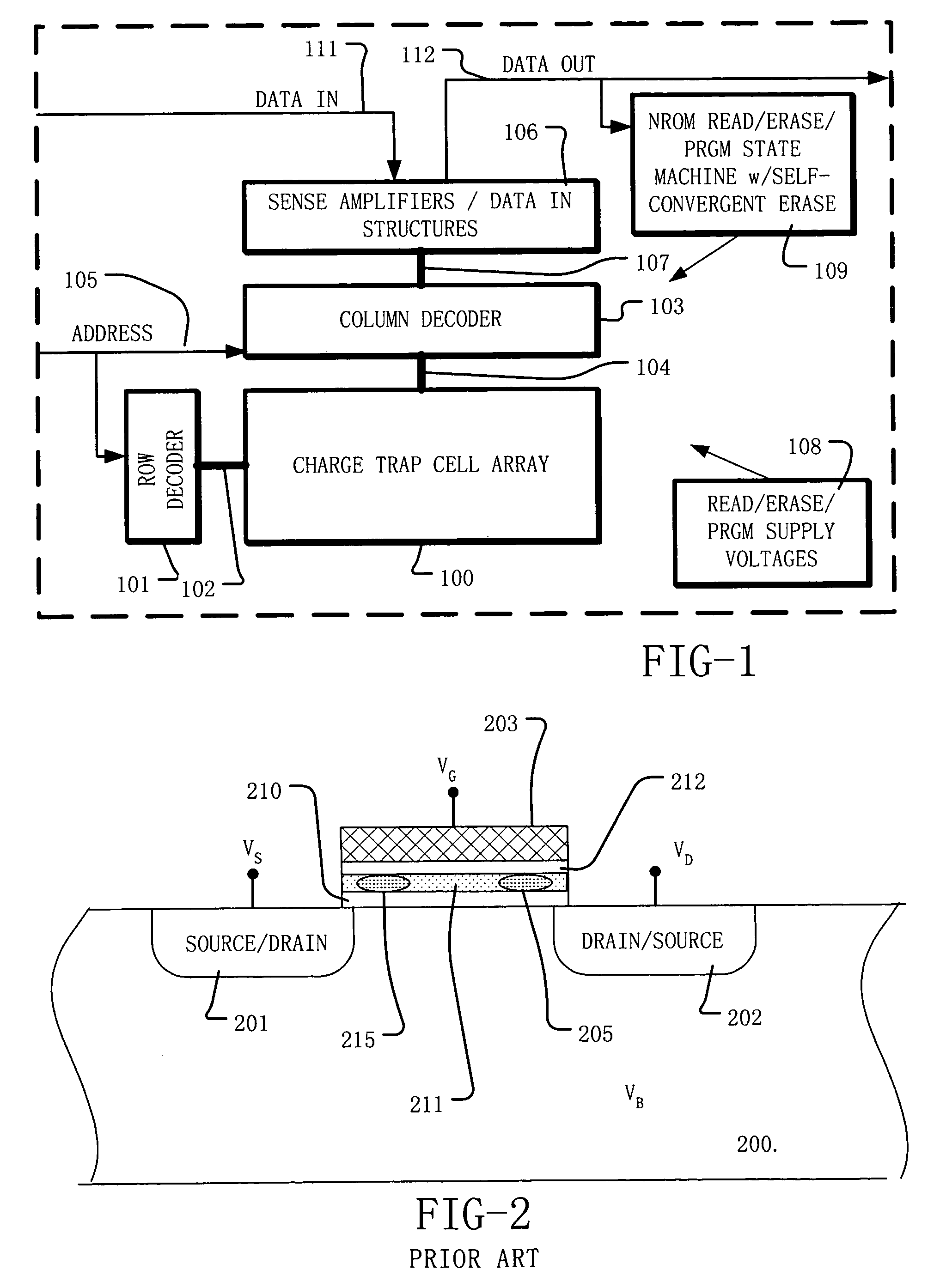
[0027]A detailed description of embodiments of the present invention is provided with reference to FIGS. 1–11.
[0028]FIG. 1 is a simplified block diagram of an integrated circuit supporting self-convergent erase according to the present invention. The integrated circuit includes a memory array 100 implemented using NROM memory cells, or other charge trapping memory cells. A page-row decoder 101 is coupled to a plurality of word lines 102 arranged along rows in the memory array 100. A column decoder 103 is coupled to a plurality of bit lines 104 arranged along columns in the memory array 100. Addresses are supplied on bus 105 to column decoder 103 and page / row decoder 101. Sense amplifiers and data-in structures in block 106 are coupled to the column decoder 103 via data bus 107. Data is supplied via the data-in line 111 from input / output ports on the integrated circuit to the data-in structures in block 106. Data is supplied via the data-out line 112 from the sense amplifiers in bloc...
PUM
 Abstract
Description
Claims
Application Information