Chamfered freestanding nitride semiconductor wafer and method of chamfering nitride semiconductor wafer

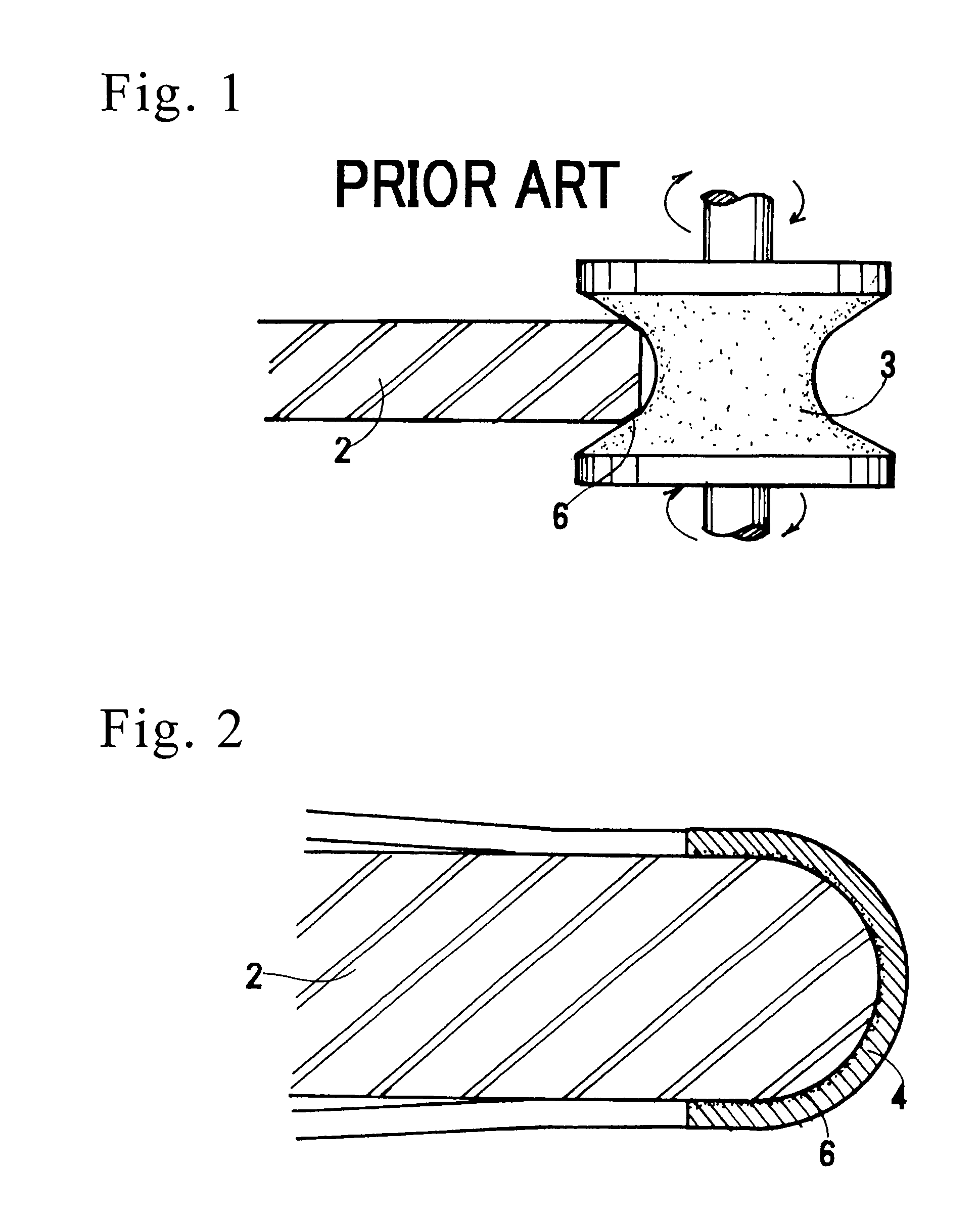
a technology of chamfering and semiconductor wafers, which is applied in the direction of manufacturing tools, semiconductor/solid-state device details, edge grinding machines, etc., can solve the problems of impulsive contact with hard rotary whetstones, high crack occurrence rate, and raised silicon chamfering cost. , to achieve the effect of reducing the crack occurrence ra

Inactive Publication Date: 2007-03-27
SUMITOMO ELECTRIC IND LTD
View PDF16 Cites 10 Cited by
  • Summary
  • Abstract
  • Description
  • Claims
  • Application Information

AI Technical Summary

Benefits of technology

[0019]The present invention proposes a nitride semiconductor wafer having an edge bevelled to roughness Ra smaller than Ra 5 μm but larger than Ra 10 nm (10 nm≦Ra≦5 μm). The roughness less than Ra 5 μm enables the nitride wafer to reduce a crack occurrence rate under 50%.
[0020]More favorably, the present invention proposes a nitride semiconductor wafer with a smooth edge bevelled to roughness Ra smaller than Ra 1 μm but larger than Ra 10 nm (10 nm≦Ra≦1 μm). The edge roughness less than Ra 1 μm allows the wafer to decrease a crack occurrence rate under 10%.
[0021]Furthermore, the present invention proposes a edge roughness less than Ra 0.1 μm for a nitride semiconductor wafer. The small roughness less than Ra 0.1 μm can suppress a crack occurrence rate under 6%.

Problems solved by technology

{circumflex over (2)} complained that silicon wafers were too rigid and resistant to mechanically bevel and diamond whetstones should be used for silicon bevelling which raised the cost of silicon chamfering.
However, the yield of chamfering is low.
Impulsive contact with the hard rotary whetstone is often destructive for the wafer.
But, such smoothness less than Ra 5 μm is beyond the power of the metal-bonded circumscribing rotary whetstone rotating at an ordinary speed.
However, the slow whetting has drawbacks of excess dissipation of whetstones, jamming of meshes with dust and big fluctuation of final properties of the wafer.
The long-time whetting is not practical for giving mirror smoothness to GaN wafers.
GaN wafers are rigid but fragile.
It is, however, difficult to finish GaN wafers due to the fragility.
However, employment of smaller-sized whetting granules requires longer time for polishing edges of wafers, which raises cost of edge polishing.
Use of the fine granule whetstones has other drawbacks of raising the probability of cramming meshes with whetting wastes and shortening the lifetime of whetstones.

Method used


Image

  • Chamfered freestanding nitride semiconductor wafer and method of chamfering nitride semiconductor wafer
  • Chamfered freestanding nitride semiconductor wafer and method of chamfering nitride semiconductor wafer
  • Chamfered freestanding nitride semiconductor wafer and method of chamfering nitride semiconductor wafer

Examples


embodiment

[Embodiment]

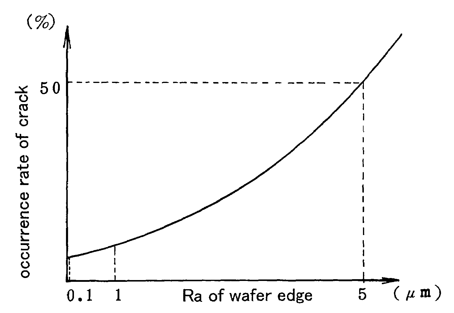
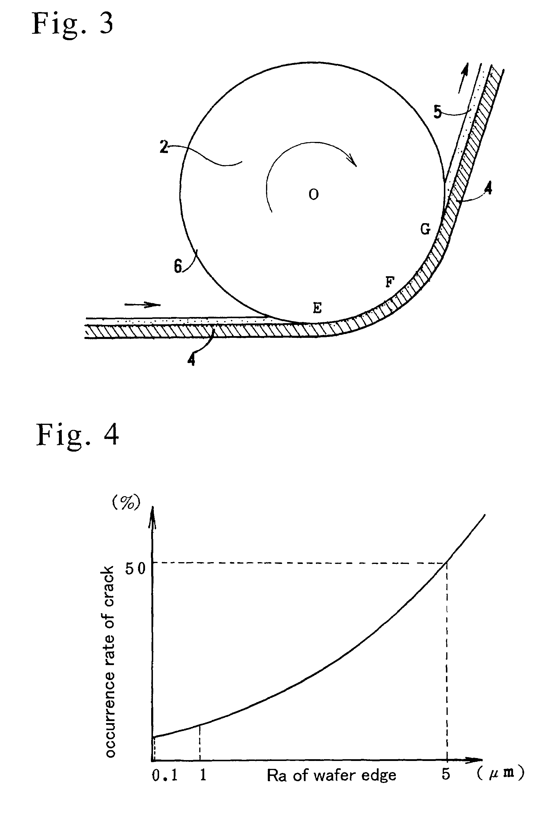
[0055]A starting wafer is an as-grown GaN wafer of a 52 mm diameter and a 520 μm thickness. An orientation flat (OF, 16 mm of a final length) and an identification flat (IF, 7 mm of a final length) are formed on sides of the GaN wafer by, for example, a dicer. FIG. 5 shows a plan view of the object GaN wafer for showing sizes of the wafer. A 52 mmφ outer full circle denotes an original size of the object wafer before edge-polishing. A left straight line shows a cutting line for the IF formation. A bottom straight line denotes a cutting line for the OF formation. A 1 mm wide edge part is eliminated by the edge polishing. A 50 mmφ inner circle shows the edge-polished wafer. Since a 1 mm wide peripheral circular part is eliminated, the lengths of the left IF line and the bottom OF line are reduced to the predetermined lengths of 7 mm and 16 mm.

[0056]The original 52 mmφ wafer is fixed to a chuck of a rotor by aligning centers. At a first bevelling step, an endless gross whet...


PUM

PropertyMeasurementUnit
contact angleaaaaaaaaaa
speedsaaaaaaaaaa
Raaaaaaaaaaa

Abstract

Technology of making freestanding gallium nitride (GaN) wafers has been matured at length. Gallium nitride is rigid but fragile. Chamfering of a periphery of a GaN wafer is difficult. At present edges are chamfered by a rotary whetstone of gross granules with weak pressure. Minimum roughness of the chamfered edges is still about Ra 10 μm to Ra 6 μm. The large edge roughness causes scratches, cracks, splits or breaks in transferring process or wafer process. A wafer of the present invention is bevelled by fixing the wafer to a chuck of a rotor, bringing an edge of the wafer into contact with an elastic whetting material having a soft matrix and granules implanted on the soft matrix, rotating the wafer and feeding the whetting material. Favorably, several times of chamfering edges by changing the whetting materials of smaller granules are given to the wafer. The chamfering can realize small roughness of Ra 10 nm and Ra 5 μm at edges of wafers.

Description

BACKGROUND OF THE INVENTION[0001]1. Field of the Invention[0002]This invention relates to an improvement of an edge (periphery) of a nitride semiconductor single crystal circular wafer. The edge means a periphery of a wafer. An as-cut wafer has a sharp edge which causes break, crack, split, chip or scratch of the wafer. Then, the edge part is slantingly polished into a round periphery. The slanting polishing of edges is called “bevelling” or “chamfering” for discriminating the edge slanting polishing from flat polishing of wafer surfaces. Semiconductor nitrides mean gallium nitride (GaN), indium nitride (InN) and aluminum nitride (AlN). The nitrides are rigid but fragile materials. Processing of semiconductor nitride wafers is far more difficult than silicon (Si) wafers or gallium arsenide (GaAs) wafers.[0003]This application claims the priority of Japanese Patent Application No. 2003-98979 filed on Apr. 2, 2003 and Japanese Patent Application No. 2003-275935 filed on Jul. 17, 2003,...

Claims


Application Information

Patent Timeline
Patent Type & Authority Patents(United States)
IPC IPC(8): B24B1/00B24B9/00B24B9/06B24B21/00H01L21/304
CPCB24B9/065B24B21/002H01L21/02021B24B9/00H01L21/304H01L29/0657
Inventor NAKAYAMA, MASAHIROIRIKURA, MASATO
Owner SUMITOMO ELECTRIC IND LTD
Why Eureka
Try Eureka