Edge card connector assembly with keying means for ensuring proper connection

a technology of connector assembly and connector housing, which is applied in the direction of coupling device connection, two-part coupling device, incorrect coupling prevention, etc., can solve the problems of difficult to retain all of the mechanical functions of the connector, and the difficulty of controlling the impedance by modifying the spacing and size of the terminals in the connector housing

Active Publication Date: 2007-04-03
MOLEX INC
View PDF29 Cites 57 Cited by
  • Summary
  • Abstract
  • Description
  • Claims
  • Application Information

AI Technical Summary

Benefits of technology

[0006]Accordingly, it is a general object of the present invention to provide a low profile connector in which the terminals may have varying shapes for controlling the impedance of the connector and in which the connector housing includes means for orienting an opposing connector for mating with the connector housing.
[0007]Another object of the present invention to provide a surface mount style connector for mounting on a circuit board, the connector having a plurality of conductive terminals supported therein in spaced apart order, the terminals having stubs formed as part thereof, thereby reducing and / or increasing the amount of metal to influence the capacitance and / or the inductance of the terminals and control the impedance thereof.
[0010]Another object of the present invention is to provide a high speed connector having an insulative housing with defined top, bottom and side surfaces, the connector housing accommodating a plurality of conductive terminals that are inserted into terminal-receiving cavities disposed in the top and bottom surfaces of the connector housing, the bottom surface of the connector housing being configured to define a recess between it and a top surface of a circuit board to which the connector housing may be mounted, the recess being sized sufficiently to receive a projection from an opposing mating connector to thereby provide a means for ensuring proper engagement between the connector housing and the opposing mating-connector, without adversely affecting the structural integrity of the connector.
[0012]A still other object of the present invention is to provide a receptacle connector that has a housing with a contacts inserted into it from the bottom face, and a hollow cavity defined along the bottom of the connector housing which accommodates a projection from a mating plug connector, the projections serving in effect as a cover to the bottom contacts when the plug connector is mated to the receptacle connector, the cover of the plug connector protecting the bottom contacts of the receptacle connector from electrostatic discharge (ESD) and also preventing the contacts from acquiring contaminants during handling.
[0018]The connector housing may include two base portions which are spaced lengthwise apart from each other. Each of these base portions preferably supports a single set of terminals near the tail portions thereof. With this arrangement, the bottom of the connector housing may be hollowed out to form a recess that opens to the front of the connector and which is closed of by one of the two base portions at the rear of the recess. This recess is configured to receive a projection from an opposing mating connector in the form of a plug connector. This recess permits a user to ensure that the opposing mating connector will be properly inserted into and mated with the connectors of the invention. This recess does not reduce the overall structural integrity of the connectors of the invention, and the location of the slots that receive the retention members also does not reduce the structural integrity of the connectors of the invention.

Problems solved by technology

However, low profile connectors, such as those used in SFP (Small Form Factor Pluggable) and SFP-like applications are desired in electronic devices in which space is a premium and thus it is difficult to control the impedance by modifying the spacing and size of the terminals in a reduced-size connector housing.
When the terminals are modified, it becomes difficult to retain all of the mechanical functions of the connector, such as terminal retention and engagement while tuning the impedance of the connector.
It is also difficult, due to the small size of the SFP-style connectors to provide the connector with some sort of keying function that will ensure proper mating with an opposing mating connector.

Method used


Image

  • Edge card connector assembly with keying means for ensuring proper connection
  • Edge card connector assembly with keying means for ensuring proper connection
  • Edge card connector assembly with keying means for ensuring proper connection

Examples


first embodiment

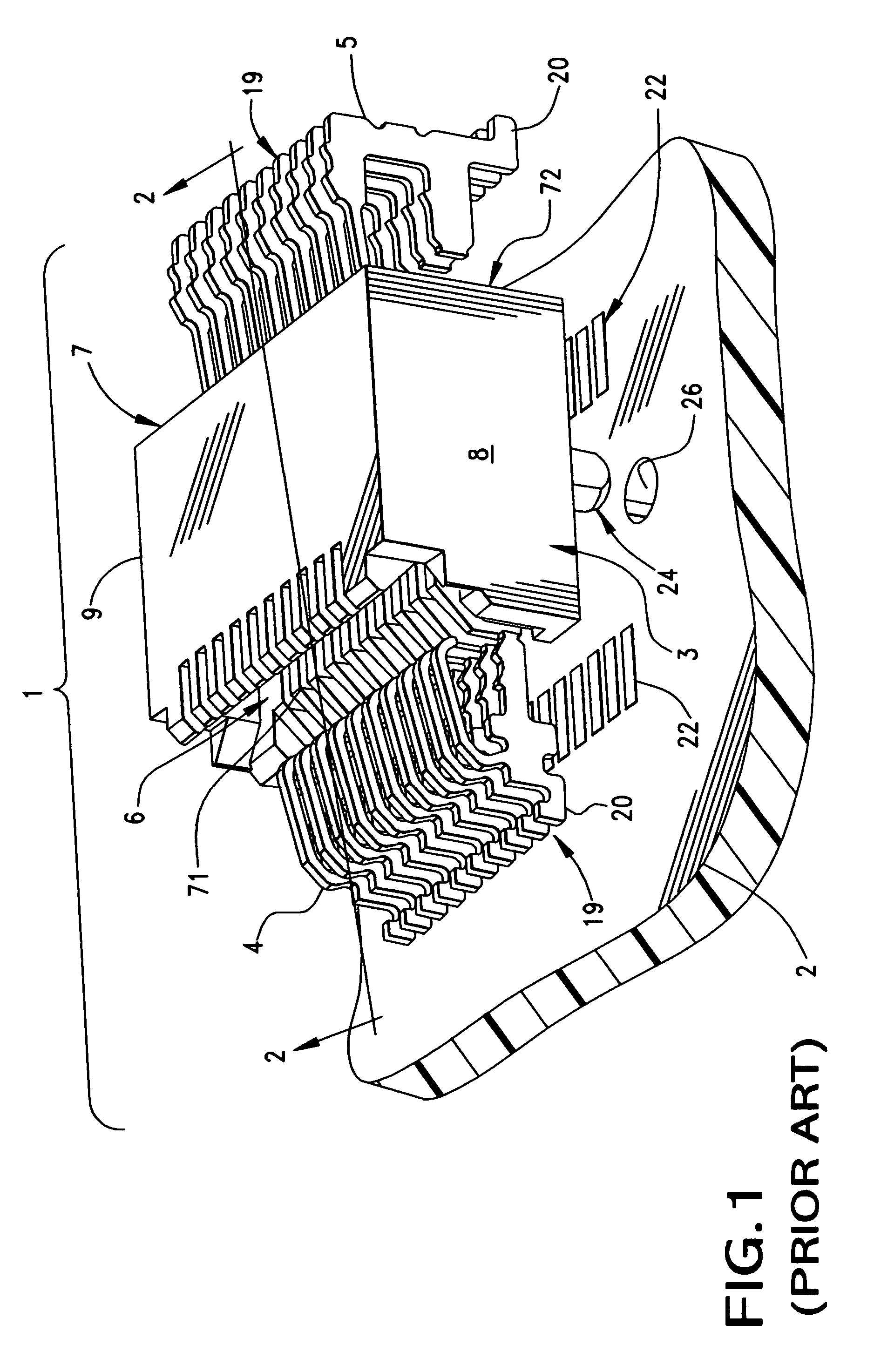
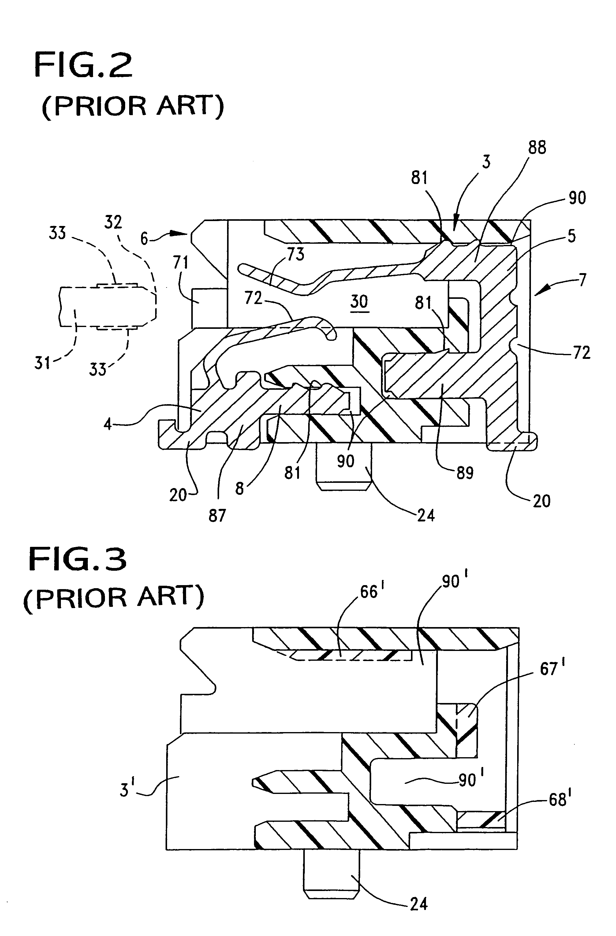
[0055]FIGS. 10–16 illustrate a connector constructed in accordance with the principles of the present invention. In this embodiment, the terminal configuration and arrangement have been changed in order to carry high speed data signals at speeds of at least approximately 2 gigabits per second and greater up to at least 10 gigabits per second and beyond. It has been found in other connectors, especially those known connectors as exemplified by FIG. 2, that certain structural elements adversely affect the ability to carry high speed signals. Mostly, it is due to at least one of the connector terminals, and such a terminal is shown by the first or front terminal 4. The large surface mount portion 20 thereof adds inductance to the overall impedance of such a connector and thus the terminal 4 must act as a low speed terminal.

[0056]The connectors of this embodiment provide the ability to carry high speed data signals of 2 GBps and greater and approaching approximately 10 GBps. As illustra...

embodiment 200

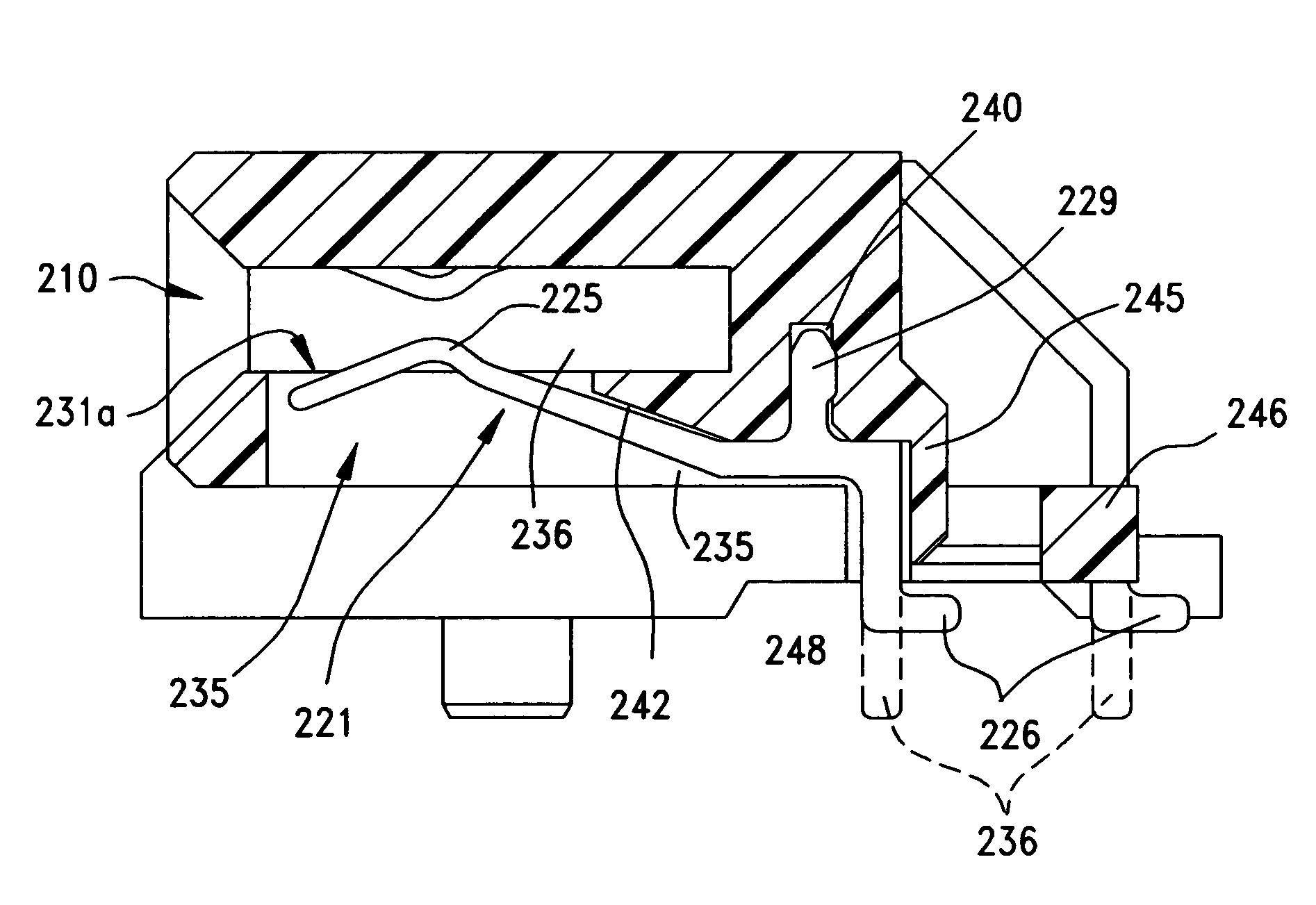
[0067]The connector housing 201 may also include, as shown in the Figures, a hollow area 260 in the form of a recess, that defines a lengthwise slot or cavity 261 underneath the card-receiving slot 210. This slot 261, as shown best in FIGS. 14–16, extends underneath and past the inward extent of the card-receiving slot 210 to a point where, as shown in the connector embodiment 200 of the invention, the recess 260 extends past the beginning of the card slot rear wall 213. Thus, in the illustrated embodiment, the card-receiving slot 210 has an insertion depth less than that of the recessed slot 261. As shown in FIG. 15, the bottom terminal row tail slots 248 open to this hollow recess 260. Because the bottom row of terminals 221 are inserted directly from the bottom of the connector, the recess 260 may be formed in the connector housing without fear of adversely affecting the structural integrity of the connector 200.

[0068]As shown in FIG. 14, the slot 261 defined by the recess will a...


PUM


Abstract

A surface mount connector for high speed data transfer application has an insulative housing with a circuit card-receiving slot disposed along a front face thereof. A plurality of conductive terminals are supported by the housing so that contact portions of the terminals extend into the card slot. The terminals are supported on opposite faces of the connector housing, specifically the top and bottom faces thereof, and each of the terminals includes a tail portion, a contact portion and a retention portion that engages the connector housing so that the contact portions are cantilevered in their extent within the housing. The housing includes a hollow recess formed on its bottom that opens to the front of the connector housing. This recess serves as a keyway that may receive a male portion of an opposing mating connector to ensure the mating connector is oriented properly before engagement.

Description

REFERENCE TO RELATED APPLICATIONS[0001]This application claims priority from U.S. Provisional Patent Application No. 60 / 586,488, filed Jul. 7, 2004.BACKGROUND OF THE INVENTION[0002]The present invention is directed generally to edge card connectors and, more specifically to edge card connectors in which the connector impedance may be controlled by shaping of the connector terminals and in which the connector includes a means for ensuring proper connection with an opposing, mating connector.[0003]High speed data transfer systems require electrical connectors in which the electrical impedance can be controlled in order to maintain the required data transfer rate of the electrical system. It is desirable at high speed data transfer rates to obtain a specific impedance in a connector that matches the impedance of the entire electronic system, i.e., the circuits on a circuit board of an electronic device and either the circuits of opposing electronic device or in a transmission cable. Th...

Claims


Application Information

Patent Timeline
Patent Type & Authority Patents(United States)
IPC IPC(8): H01R24/00H01R12/71
CPCH01R23/7073H01R12/725H01R12/57H01R13/64H01R12/721
Inventor REGNIER, KENTNEER, JAY H.
Owner MOLEX INC
Why Eureka
Try Eureka