Conductive film, method of producing the same, and touch panel

a technology of conductive film and touch panel, which is applied in the direction of conductive layers on insulating supports, instruments, photosensitive materials, etc., can solve the problems of yellowish reflected light of external light and color of reflected light of a white light source, and achieve excellent conductive characteristics and hardly visible effects

Active Publication Date: 2019-06-25
FUJIFILM CORP
View PDF9 Cites 0 Cited by
  • Summary
  • Abstract
  • Description
  • Claims
  • Application Information

AI Technical Summary

Benefits of technology

[0006]As a method of lowering the volume resistivity of a thin conductive wire, there is a method of increasing the amount of a metal portion in a thin conductive wire. On the other hand, since visible light is strongly reflected due to the characteristics of metal in such a thin conductive wire, the thin conductive wire is easily viewed. Particularly, in order to apply the thin conductive wire to a detection electrode of a touch panel (sensor electrode), in a case in which a mesh pattern formed by the thin conductive wire is prepared, the reflectivity of external light peculiar to metal is increased and the mesh pattern is easily viewed. Further, in a case in which the main component of the metal portion included in the thin conductive wire in the mesh pattern is silver, there arise problems that the reflected light of external light is yellowish and the reflected light of a white light source seems to be colored due to plasmon resonance caused by the fine structure of the silver.
[0010]As a result of conducting intensive investigations on the above problems, the present inventors have found that it is possible to obtain a desired effect by controlling a distribution state of a metal portion in a thin conductive wire.
[0040]According to the present invention, it is possible to provide a conductive film having a thin conductive wire which has excellent conductive characteristics and is hardly visible, and a method of producing the same.

Problems solved by technology

Further, in a case in which the main component of the metal portion included in the thin conductive wire in the mesh pattern is silver, there arise problems that the reflected light of external light is yellowish and the reflected light of a white light source seems to be colored due to plasmon resonance caused by the fine structure of the silver.
That is, a trade-off relation between improvement of the conductive characteristics of the thin conductive wire and difficulty in visibility thereof is established in many cases and it is required to satisfy the both at a higher level.

Method used


Image

  • Conductive film, method of producing the same, and touch panel
  • Conductive film, method of producing the same, and touch panel
  • Conductive film, method of producing the same, and touch panel

Examples


first embodiment

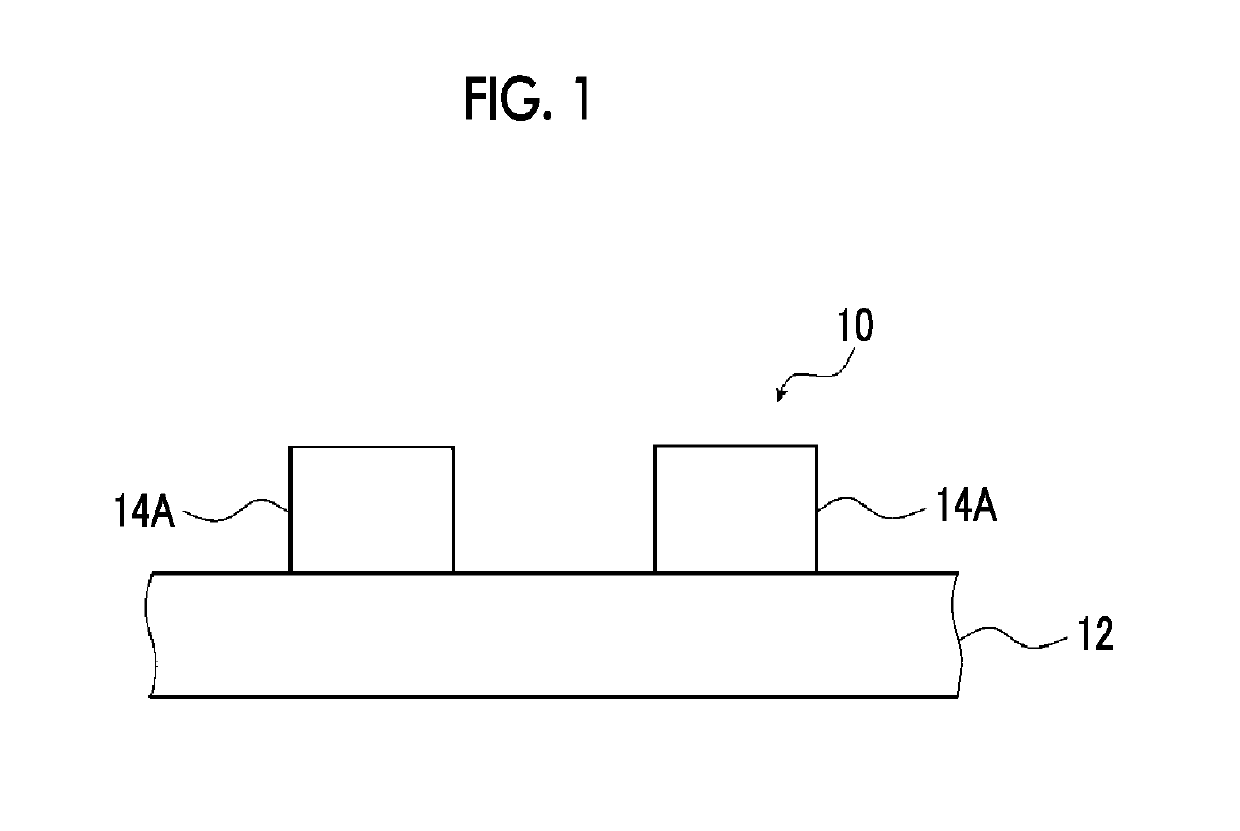
[0053]Hereinafter, the first embodiment of the conductive film of the present invention will be described with reference to the drawings.

[0054]FIG. 1 shows a cross-sectional view of the first embodiment of the conductive film of the present invention.

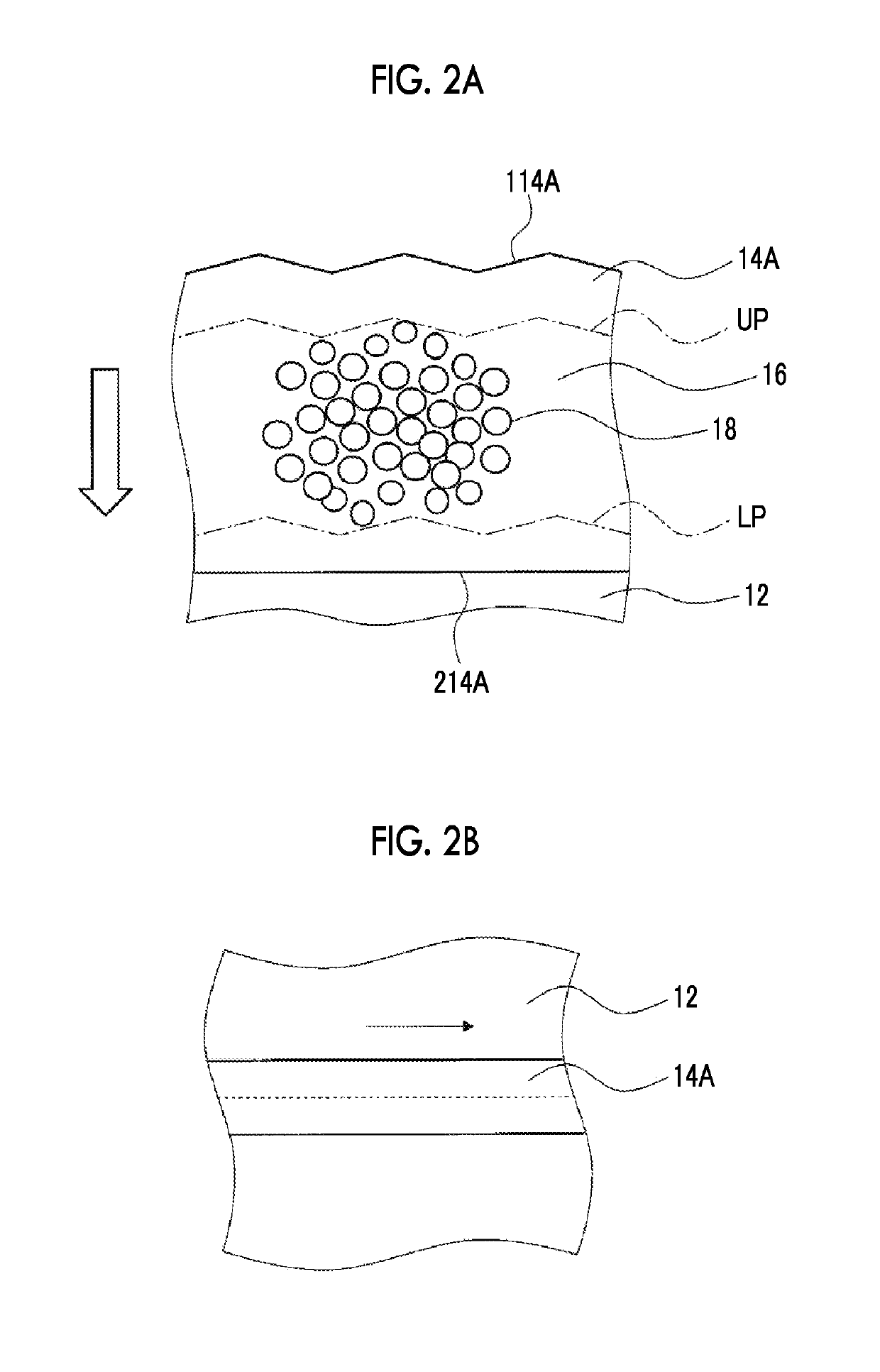
[0055]A conductive film 10 includes a support 12, and a thin conductive wire 14A that IS arranged on the support 12. In FIG. 1, two thin conductive wires 14A are shown but the number of conductive wires is not particularly limited.

[0056]FIG. 2A shows a partially enlarged cross-sectional view of the thin conductive wire 14A. The thin conductive wire 14A includes a polymer 16, and a plurality of metal portions 18 dispersed in the polymer 16. As shown in FIG. 2A, the amount of the metal portion 18 distributed is small in a region near a surface 114A side of the thin conductive wire 14A or a region near a surface 214A and the amount of the metal portion distributed near the middle region in the thin conductive wire 14A is large.

[0057]In the...

modification examples

[0185]As a modification example of Method 1, an embodiment in which in the above-described first step, the composition adjusted coating liquid, the silver halide-containing coating liquid, and the composition adjusted coating liquid are applied in this order from the support side by simultaneous multilayer coating may be adopted. That is, a method in which three coating liquids are applied by simultaneous multilayer coating to provide layers having a low metal portion density on to both surfaces of the thin wire may be used.

[0186]In a case in which the simultaneous multilayer coating is performed such that the composition adjusted coating liquid, the silver halide-containing coating liquid, and the composition adjusted coating liquid are laminated in this order from the support side, a coating film B, a coating film A, and the coating film B are laminated in this order on the support and silver halide diffuses into the respective two coating films B positioned on both surfaces of th...

second embodiment

[0204]Hereinafter, the second embodiment of the conductive film of the present invention will be described with reference to the drawings.

[0205]The second embodiment of the conductive film and the above-described first embodiment have the same configuration except the method of calculating the average area ratio of metal in the thin conductive wire and thus a method of calculating the average area ratio of metal will be mainly described in detail below.

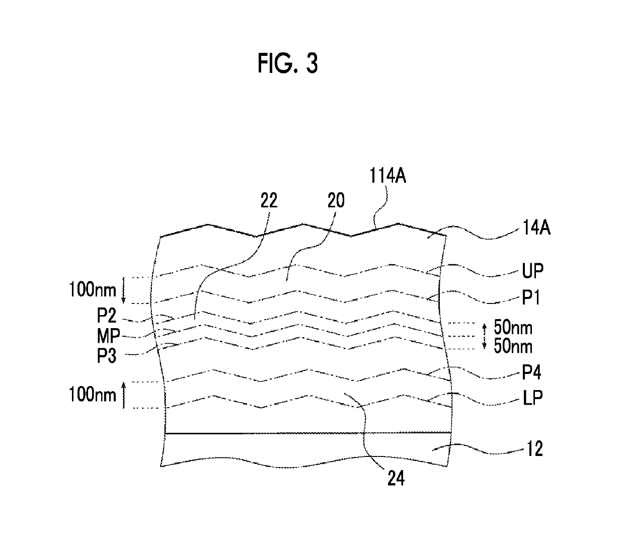
[0206]Using FIG. 6, a method of obtaining the average area ratio of the metal portion in each region in the thin conductive wire will be described in detail. FIG. 6 is a partially enlarged view of the thin conductive wire but display of the metal portion is omitted.

[0207]First, using FIG. 6, a lower end position LP and an upper end position UP used to define the distribution state of the metal portion 18 will be described.

[0208]As shown in FIG. 6, on a vertical section of a thin conductive wire 14C (a cross section in a case of cuttin...


PUM


Abstract

The conductive film is arranged on the support and contains a binder and a metal portion, in which a position at which the contour line reaches the metal portion included in the thin conductive wire is set as an upper end position, and an average area ratio VA of the metal portion in a region ranging from the upper end position to 100 nm toward the support side is 1% or more and less than 50%, and a position at which the contour line reaches the thin conductive wire does not include the metal portion is set to a lower end position, and an average area ratio VM1 of the metal portion in a region ranging from a middle position between the upper end position and the lower end position to 50 nm toward the support side and to 50 nm toward the surface X side is 50% or more.

Description

CROSS-REFERENCE TO RELATED APPLICATIONS[0001]This application is a Continuation of PCT International Application No. PCT / JP2015 / 080199 filed on Oct. 27, 2015, which claims priority under 35 U.S.C § 119 (a) to Japanese Patent Application No. 2015-069367 filed on Mar. 30, 2015. Each of the above application(s) is hereby expressly incorporated by reference, in its entirety, into the present application.BACKGROUND OF THE INVENTION1. Field of the Invention[0002]The present invention relates to a conductive film, particularly relates to a conductive film having a thin conductive wire which has excellent conductive characteristics and is prevented from being visible due to external light, and a method of producing the same. The present invention also relates to a touch panel including the conductive film.2. Description of the Related Art[0003]A conductive film in which thin conductive wires are formed on a support is widely used for an electrode for various electronic devices such as a sol...

Claims


Application Information

Patent Timeline
Patent Type & Authority Patents(United States)
IPC IPC(8): G03C1/04G06F3/044G03C1/74G03C1/46H01B5/14G03C1/053H01B1/02H01B13/00
CPCH01B5/14G03C1/053G03C1/46G03C1/74G06F3/044H01B13/0036H01B1/026G06F2203/04112G03C2001/041G03C2001/042G06F2203/04103
Inventor KATAGIRI, KENSUKETAJIRI, SHINFUJII, TOSHINARI
Owner FUJIFILM CORP
Why Eureka
Try Eureka