Al technical title is built by PatSnap Al team. It summarizes the technical point description of the patent document.
a memory cell and dual protection technology, applied in the field of memory cell dual protection, can solve the problems of destroying the entire operation, dram cell, degrading its stability, etc., and achieve the effects of safe route, easy scaling down, and higher yield memory array
Inactive Publication Date: 2007-04-17
MIRADIA INC
View PDF63 Cites 7 Cited by
Summary
Abstract
Description
Claims
Application Information
AI Technical Summary
This helps you quickly interpret patents by identifying the three key elements:
Problems solved by technology
Method used
Benefits of technology
Benefits of technology
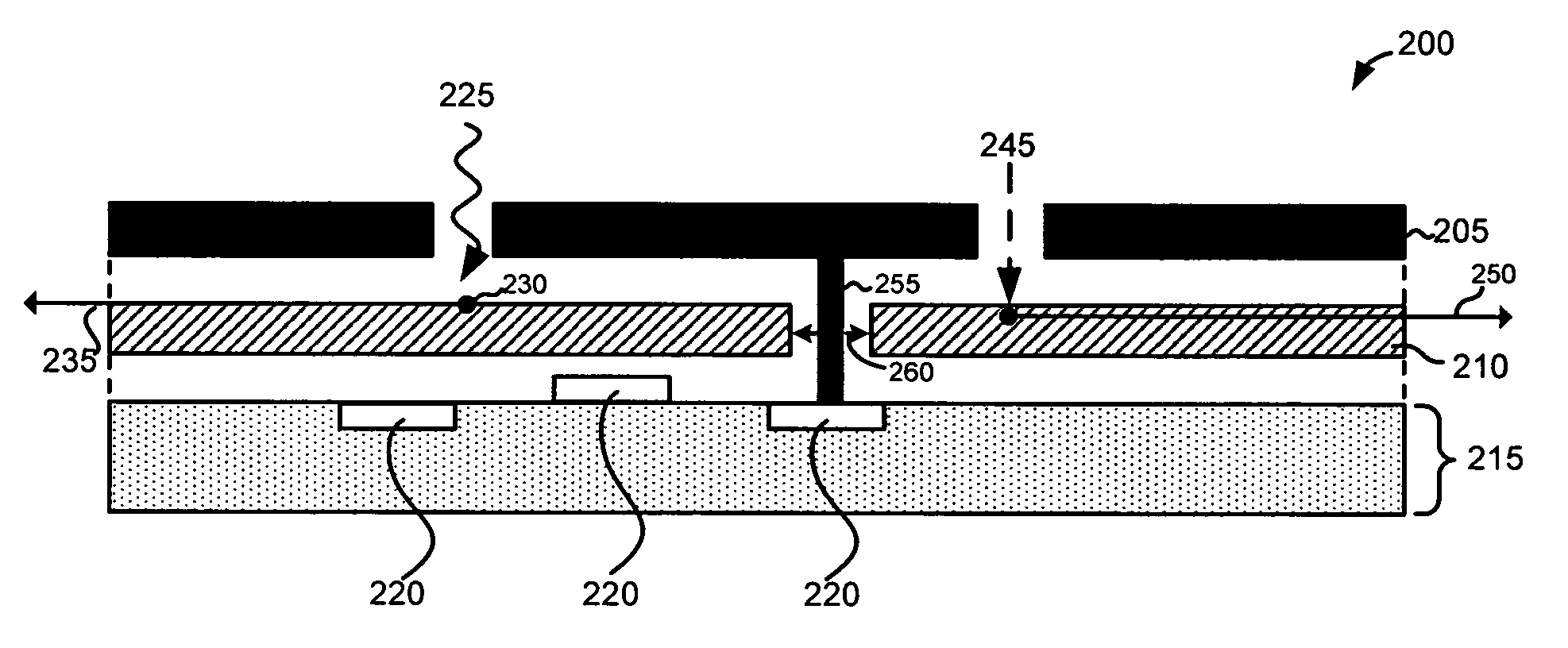
[0010]The present invention relates to a process and apparatus for protecting memory cells from the effects of both incident light and electrical noise. Embodiments in accordance with the present invention provide multiple types of protection using a single layer with a dual purpose. A layer of the device made up of metal normally used for chip-level signal routing is used as a dedicated ground plane shaped to approximate the cell.
[0011]Digital micro-mirrors operate under the extreme environment of high photon flux. Without any protection, an incident photon can hit the silicon substrate and create an electron-hole pair. The subsequent diffusion of the photo-generated electrons and holes into the active transistor region changes the charge state of the DRAM cell and degrades its stability.
[0013]Unlike conventional devices, the ground plane utilized in one embodiment of the present invention is not connected to any of the electrodes. As a result, the ground plane is not affected by the bias switching of the micro-mirrors. In addition, the shielding currents in the ground plane protect the SLM from the electrical field disturbance induced by the switching mirror bias voltage. The current is then returned to the source of the switching bias voltage. Conservation of charge requires such a return current, however, without the use of a ground plane as the path of least resistance, the return current would traverse the memory array itself, disrupting its operation or destroying it entirely. Thus, embodiments of the present invention allow for the return current to traverse the ground plane instead, and the current is safely routed out of the chip.
[0014]The present invention employs a DRAM-based approach, which employs a higher yield memory array that more easily scales down to smaller pixel sizes. The smaller size translates into an intrinsic yield enhancement over SRAM-based approaches. Ultimately, this approach provides significant cost savings over SRAM-based approaches.
Problems solved by technology
The subsequent diffusion of the photo-generated electrons and holes into the active transistor region changes the charge state of the DRAM cell and degrades its stability.
Conservation of charge requires such a return current, however, without the use of a ground plane as the path of least resistance, the return current would traverse the memory array itself, disrupting its operation or destroying it entirely.
Method used
Image
Click on the blue label to locate the original text in one second.
Reading with bidirectional positioning of images and text.
Examples
Embodiment Construction
System Architecture
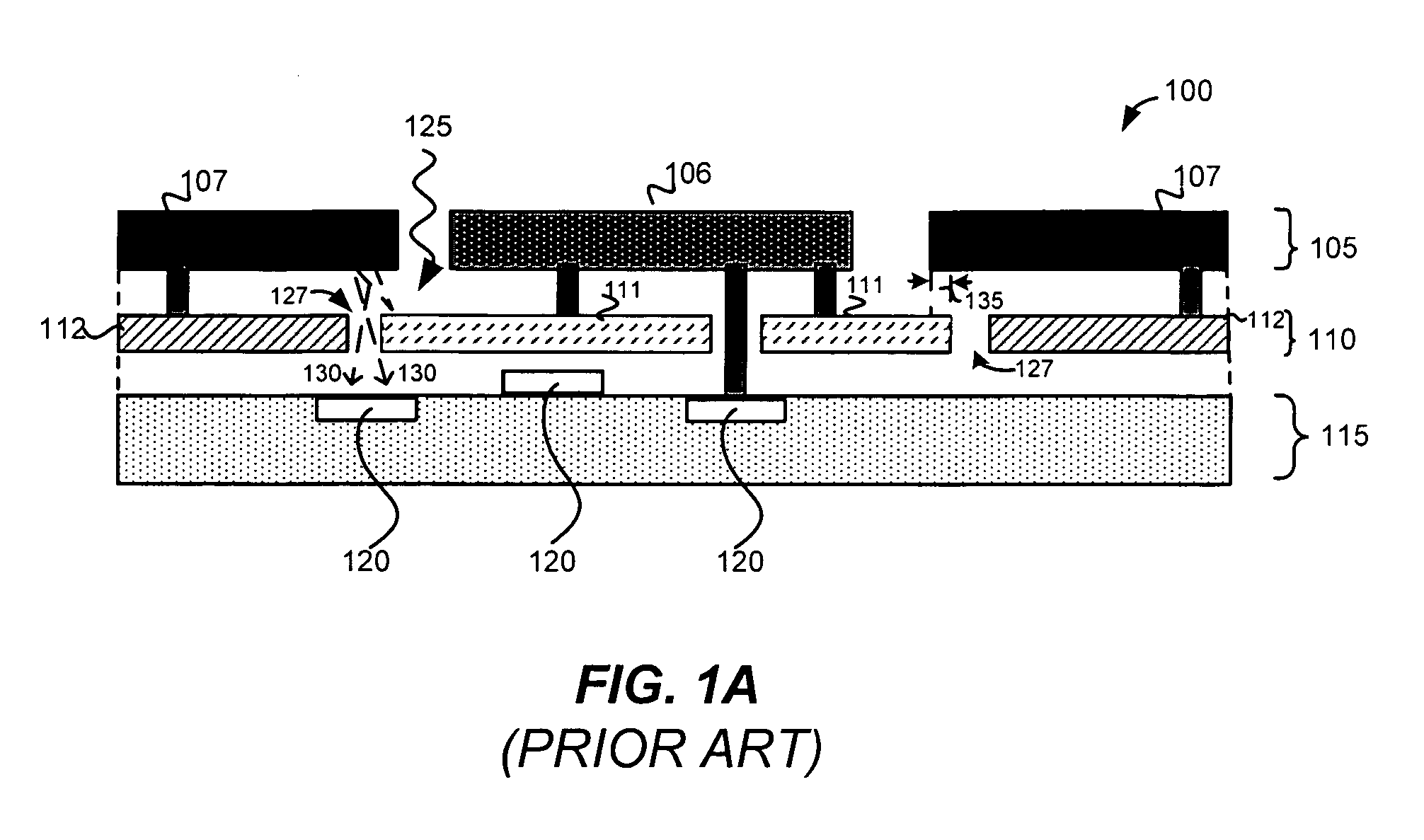
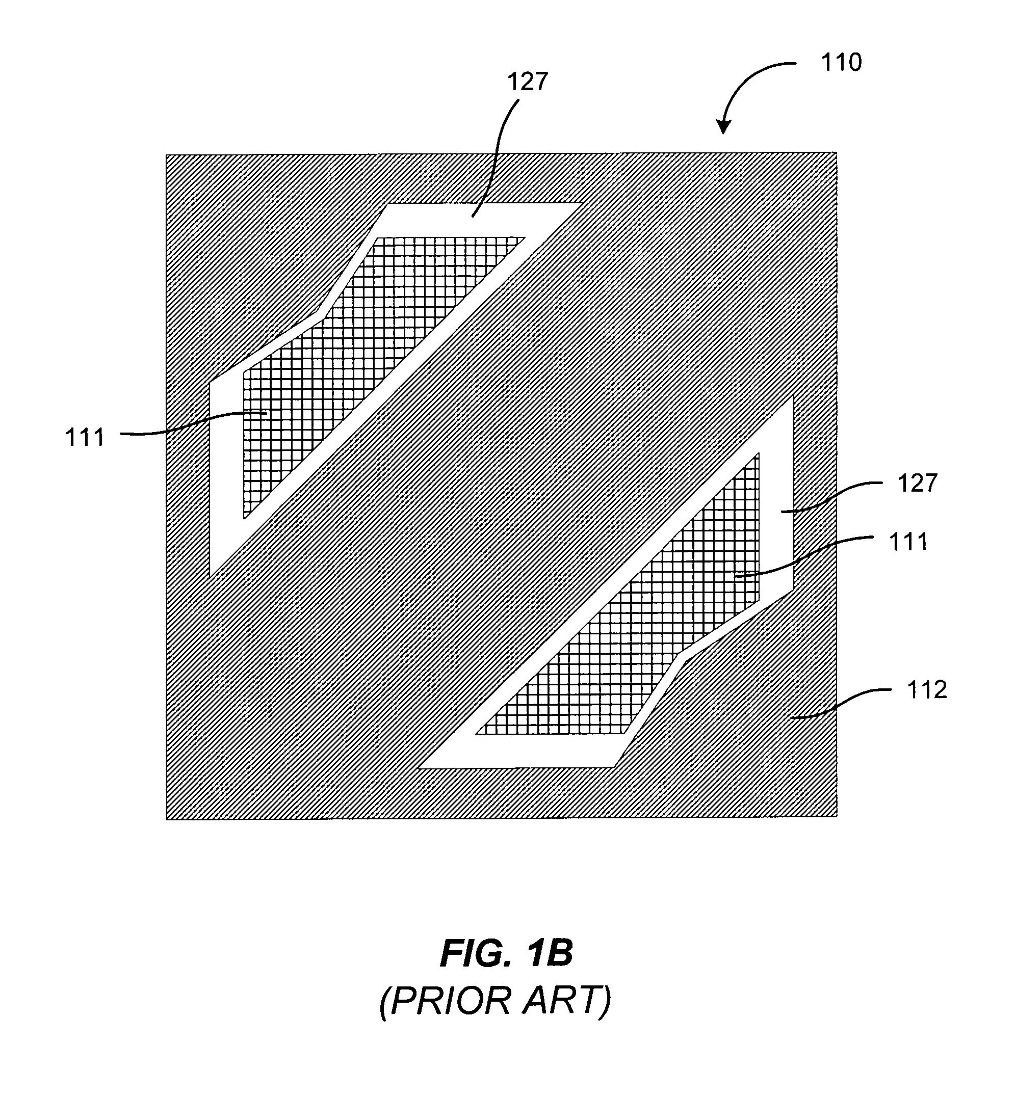
[0021]Referring now to FIG. 1A, there is shown a cross-sectional view of a conventional spatial light modulator (SLM) 100. The SLM 100 includes an electrode layer 105, with an addressing electrode 106 and landing electrodes 107, a two-region light blocking layer 110, with regions 111 electrically connected to the addressing electrode 106 and regions 112 electrically connected to the landing electrodes 107, and a device layer 115 with electrically active regions 120, such as a source, gate, and drain. Referring now also to the top plan view of the conventional two-region light-blocking layer 110 of FIG. 1B, it is comprised of metal or another opaque material and is designed to block incident light 125 from impinging on the device layer 115. However, gaps 127 between the regions of the layer 110 allow some light to pass through. As incident light 125 hits the light-blocking layer 110, light 125 is blocked from impinging directly in the device layer 115. However, the...
PUM
Property
Measurement
Unit
electrically conductive
aaaaa
aaaaa
light energy
aaaaa
aaaaa
electrical
aaaaa
aaaaa
Abstract
A spatial light modulator for use in projection display applications is provided. The spatial light modulator includes a substrate including a plurality of electrically active circuits and an electrode layer electrically coupled to at least one of the plurality of electrically active circuits. In one embodiment, the electrode layer includes a semi-continuous layer with at least one optical path. The spatial light modulator also includes a shielding layer electrically isolated from the electrode layer and disposed between the substrate and the plurality of electrically active circuits and an electrical connector coupling the shielding layer to a reference potential. In a specific embodiment, the shielding layer of the spatial light modulator converts incident light energy to electrical current and routes the current back to a source. In another specific embodiment, the shielding layer converts electrical field disturbance to electrical current and routes the current back to a source.
Description
CROSS-REFERENCES TO RELATED APPLICATIONS[0001]This application is a continuation-in-part of U.S. patent application Ser. No. 10 / 849,364 now U.S. Pat. No. 6,992,810, entitled “High Fill Ratio Reflective Spatial Light Modulator with Hidden Hinge” and Ser. No. 10 / 849,404, entitled “Fabrication of a High Fill Ratio Reflective Spatial Light Modulator with Hidden Hinge,” both of which were filed on May 18, 2004 and both of which claim priority from U.S. Provisional Application Ser. No. 60 / 475,404, entitled “Hidden Hinge High Fill Ration Reflective Spatial Light Modulator,” filed Jun. 2, 2003, and are continuations-in-part of U.S. application Ser. No. 10 / 378,056 now abandoned, entitled “Reflective Spatial Light Modulator,” Ser. No. 10 / 378,041 now abandoned, entitled “Fabrication of a Reflective Spatial Light Modulator,” and Ser. No. 10 / 378,058 now abandoned, entitled “Architecture of a Reflective Spatial Light Modulator,” all filed Feb. 27, 2003 and all claiming priority from U.S. Provisio...
Claims
Application Information
Patent Timeline
Application Date:The date an application was filed.
Publication Date:The date a patent or application was officially published.
First Publication Date:The earliest publication date of a patent with the same application number.
Issue Date:Publication date of the patent grant document.
PCT Entry Date:The Entry date of PCT National Phase.
Estimated Expiry Date:The statutory expiry date of a patent right according to the Patent Law, and it is the longest term of protection that the patent right can achieve without the termination of the patent right due to other reasons(Term extension factor has been taken into account ).
Invalid Date:Actual expiry date is based on effective date or publication date of legal transaction data of invalid patent.
