Power-up signal generating apparatus

a power-up signal and signal generating technology, applied in the field of semiconductor design techniques, can solve the problems of deterioration of chip reliability, failure of chip initialization operation, etc., and achieve the effect of improving chip reliability

Inactive Publication Date: 2007-05-01
SK HYNIX INC
View PDF36 Cites 22 Cited by
  • Summary
  • Abstract
  • Description
  • Claims
  • Application Information

AI Technical Summary

Benefits of technology

[0022]It is, therefore, a primary object of the present invention to provide a power-up signal generating apparatus for improving chip reliability.

Problems solved by technology

As described above, the conventional power-up signal generating apparatus is so sensitive to the surrounding temperature around the semiconductor, which makes the power-up signal pwrup active at irregular levels of the power supply voltage VDD and, as a result, leads failure of initialization operation of a chip and deterioration of chip reliability.
When the power-up signal becomes active before the power supply voltage VDD rises up to a certain level due to rising of the surrounding temperature, chip initialization is failed.
On the other hand, when the activation of the power-up signal is lagged due to falling of the surrounding temperature, the semiconductor device operates abnormally in a low voltage region.

Method used


Image

  • Power-up signal generating apparatus
  • Power-up signal generating apparatus
  • Power-up signal generating apparatus

Examples


Embodiment Construction

[0028]Hereinafter, with reference to the accompanying drawings, a preferred embodiment of the present invention will be explained in detail.

[0029]In the present invention, a voltage level of a bias signal is increased when temperature rises up to reduce increase of resistance of an NMOS transistor due to rising of temperature so as to reduce impact of temperature on the power-up signal. Further, the voltage level of the bias signal is reduced when temperature falls down to reduce reduction of the resistance of the NMOS transistor due to falling of temperature. As such, the active point of the power-up signal can be adjusted.

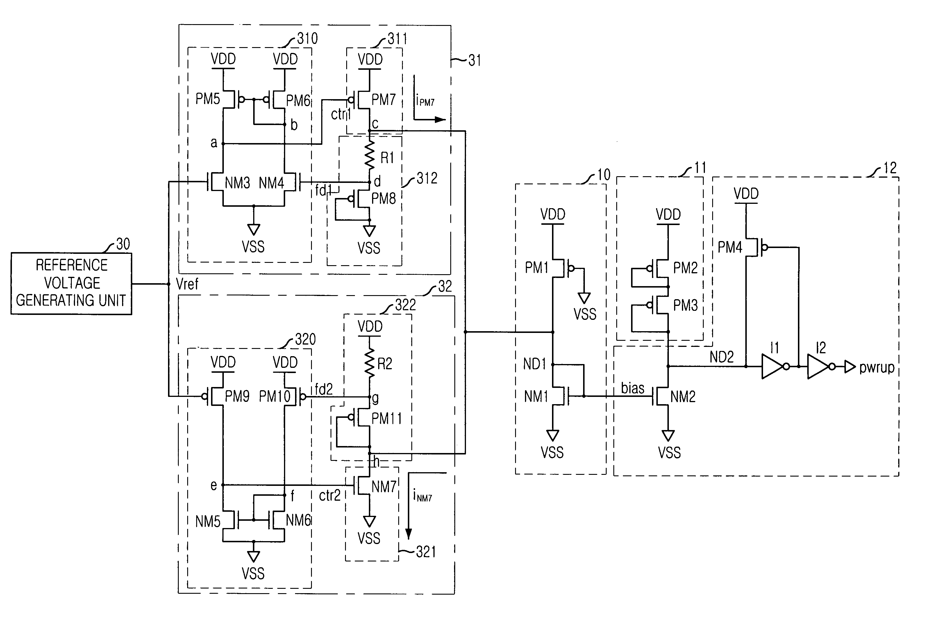
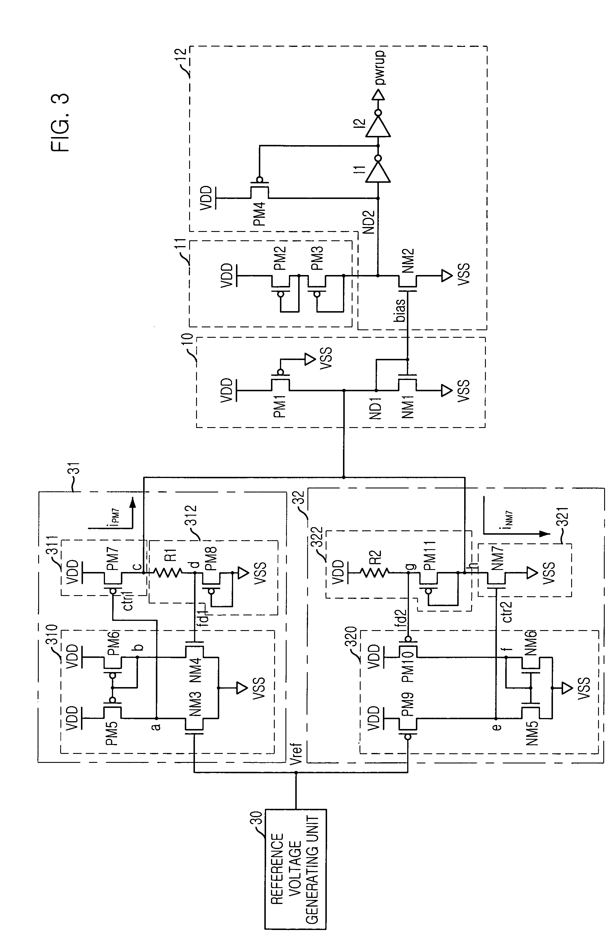
[0030]FIG. 3 represents a circuit diagram of a power-up signal generating apparatus in accordance with one embodiment of the present invention.

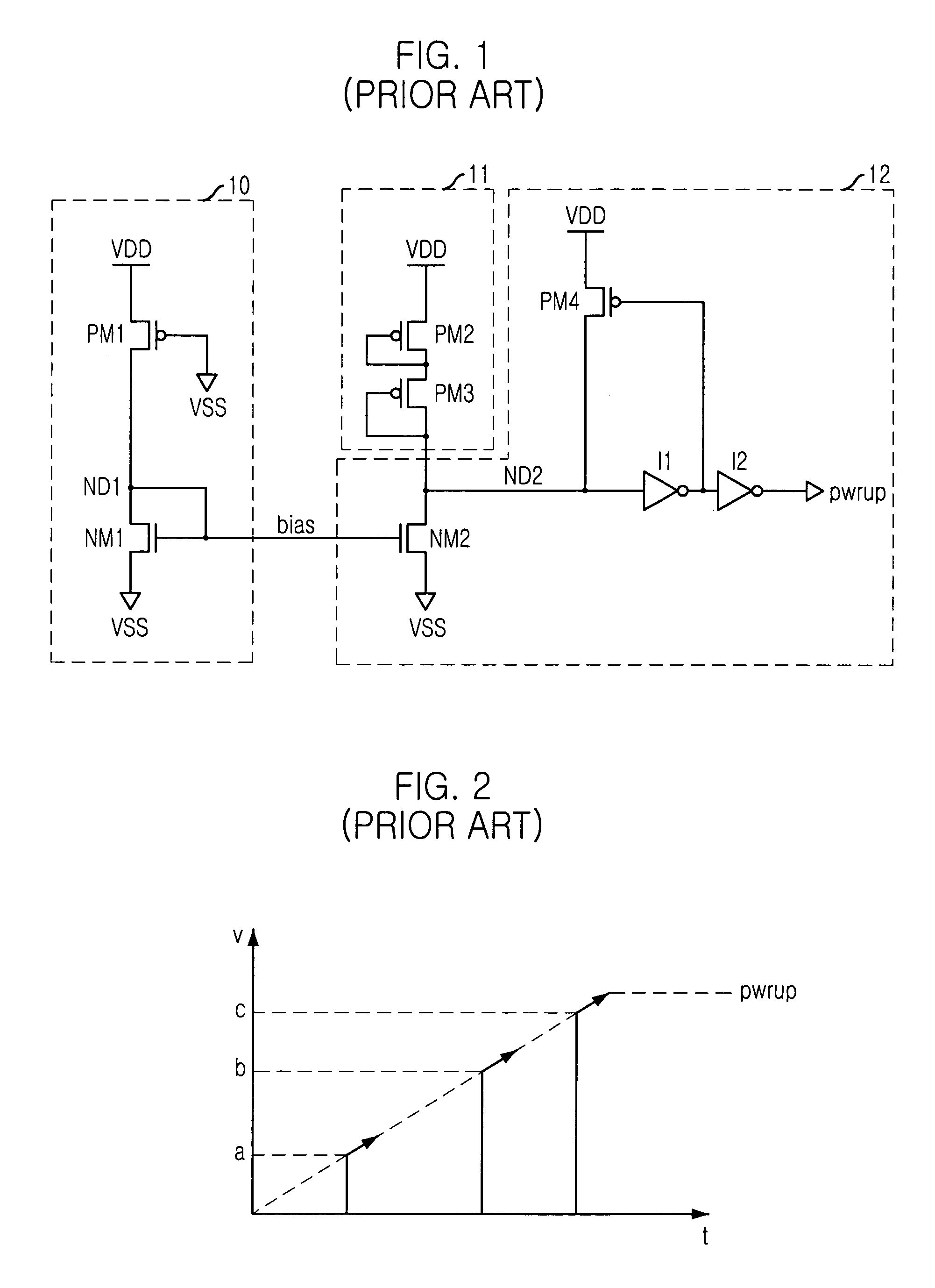
[0031]Referring to FIG. 3, the power-up signal generating apparatus comprises a reference voltage generating unit 30 for generating a reference voltage Vref, a current supplying unit 31 for receiving the reference voltage ...


PUM


Abstract

In a power-up signal generating device, a power-up signal is activated at a certain level of the power supply voltage VDD by adjusting the turn-on resistance value of the MOS transistor so that the chip reliability can be improved. The power-up signal generating device comprises a reference voltage generating unit, a bias level adjusting unit, a bias signal generating unit and a signal outputting unit. The reference voltage generating unit generates a reference voltage. The bias level adjusting unit receives the reference voltage as an input for controlling a voltage level of a bias signal in a constant level. The bias signal generating unit generates the bias signal under control of the bias level adjusting unit. The signal outputting unit outputs a power-up signal depending on the voltage level of the bias signal.

Description

FIELD OF THE INVENTION[0001]The present invention relates to semiconductor design technique; and, more particularly, to a power-up signal generating apparatus.BACKGROUND OF THE INVENTION[0002]Generally, a semiconductor memory device starts its operation after a power voltage level rises up to a certain level instead of starting in response to the level of the power voltage immediately after the power voltage is externally supplied. For this reason, the semiconductor memory device usually includes a power-up circuit.[0003]The power-up circuit prohibits the entire memory device from damaged due to latch-up when the internal circuit of the device is operated before the power voltage is stabilized after the power voltage is supplied externally so that chip level reliability can be improved. Such a power-up circuit detects the rise of the power voltage that is supplied externally when the power voltage is supplied initially so as to output a power-up signal in ‘low’ state till a certain ...

Claims


Application Information

Patent Timeline
Patent Type & Authority Patents(United States)
IPC IPC(8): H03L7/00G11C7/00G05F3/20H05B41/16
CPCG05F3/205G11C7/00
Inventor HUR, YOUNG-DO
Owner SK HYNIX INC
Why Eureka
Try Eureka