Liquid crystal display and method of manufacturing the same and method of driving the same

a liquid crystal display and liquid crystal technology, applied in non-linear optics, instruments, optics, etc., can solve problems such as collapse or defect of alignment division, interference of alignment, and easy disturbance of alignment of liquid crystal molecules, and achieve superior viewing angle characteristics

Inactive Publication Date: 2007-05-01
GOLD CHARM LTD
View PDF57 Cites 23 Cited by
  • Summary
  • Abstract
  • Description
  • Claims
  • Application Information

AI Technical Summary

Benefits of technology

[0068]Therefore, it is an object of the present invention to provide a liquid crystal display having superior viewing angle characteristics.

Problems solved by technology

Here, the first problem in the above-mentioned prior art liquid crystal display element is that disturbance of alignment which is called disclination and which is caused by lateral electric field between the wiring electrode and the pixel electrode.
The second problem in the above-mentioned prior art liquid crystal display element is that, when pressure is applied from the outside to the liquid crystal display panel having such liquid crystal display element by pressing the panel by a finger or by a pen point, alignment of liquid crystal molecules is easily disturbed, or alignment division collapses or becomes defective.
This is because, the prior art liquid crystal display panel does not have sufficient mechanical strength and cell gap of the liquid crystal display panel changes easily by the pressure applied thereto, so that alignment of the liquid crystal molecules is changed.
Also, it is impossible to easily and simply realize division of a pixel region into a plurality of domains having different alignment to obtain a wide viewing angle.
However, because of behavior peculiar to liquid crystal molecules in a condition a voltage is applied, there occurs a problem that the TN type liquid crystal display has a narrow viewing angle.
This problem of narrow viewing angle is prominent in a direction toward which liquid crystal molecules rise when medium gray is displayed.
In addition to this, there is a problem that a very precise assemble technology is required for precisely combine the upper substrate 501 and the lower substrate 507.
This problem is especially important in an active matrix type liquid crystal display which uses switching elements such as TFT's and the like.
Therefore, fabrication process becomes complicated, and a high precision alignment and assemble technology is required for the upper substrate 501 and the lower substrate 507.
In the IPS type liquid crystal display and in the liquid crystal display in which vertically aligned liquid crystal molecules are rotated down by using the lateral electric field, there is a problem that an aperture ratio is deteriorated.
Also, in these liquid crystal displays, when a cell gap of each pixel is narrowed to obtain high operating speed, a high drive voltage is required.
In the IPS type liquid crystal display and in the liquid crystal display in which vertically aligned liquid crystal molecules are rotated down by using the lateral electric field, there is still another problem as follows.
That is, in such prior art liquid crystal displays, since a color filter layer is disposed between a layer in which liquid crystal molecules are disposed and an opposing substrate, especially when switching elements are formed by using a TFT structure, an electric field produced by applying a voltage between the source electrode and the common electrode affects the color filter layer, and deteriorates display characteristics.
Therefore, such electric field affects display characteristics, especially color irregularity.
Therefore, a manufacturing process becomes complicated.

Method used


Image

  • Liquid crystal display and method of manufacturing the same and method of driving the same
  • Liquid crystal display and method of manufacturing the same and method of driving the same
  • Liquid crystal display and method of manufacturing the same and method of driving the same

Examples


embodiment 1

[Embodiment 1]

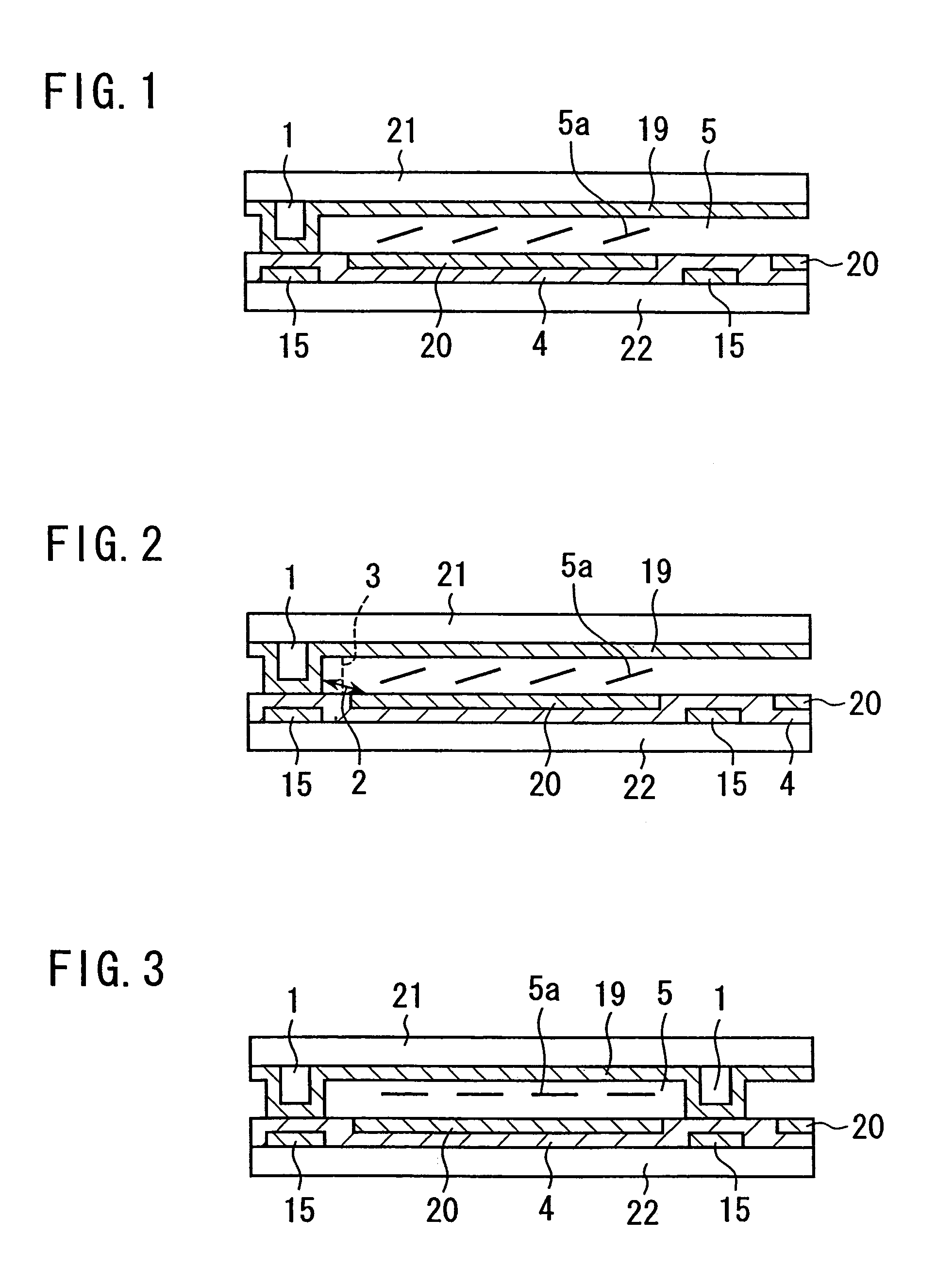
[0216]FIG. 1 illustrates a schematic cross section of a portion including approximately one pixel of a liquid crystal display element according to the first embodiment.

[0217]Referring to FIG. 1, an explanation will be made on a structure of the liquid crystal display element according to the first embodiment.

[0218]The liquid crystal display element according to the first embodiment comprises a pair of opposing transparent substrates 21 and 22, and liquid crystal material 5 filling the space between the pair of transparent substrates 21 and 22. Here, the pair of opposing transparent substrates 21 and 22 constitute an upper substrate 21 and a lower substrate 22.

[0219]The liquid crystal material 5 can be any of nematic liquid crystal material, cholesteric or chiralsmectic liquid crystal material, discotic liquid crystal material.

[0220]Operation mode of the liquid crystal material 5 may be any of TN (Twisted Nematic), STN (Super Twisted Nematic), homogeneous, homeotropic, ...

embodiment 2

[Embodiment 2]

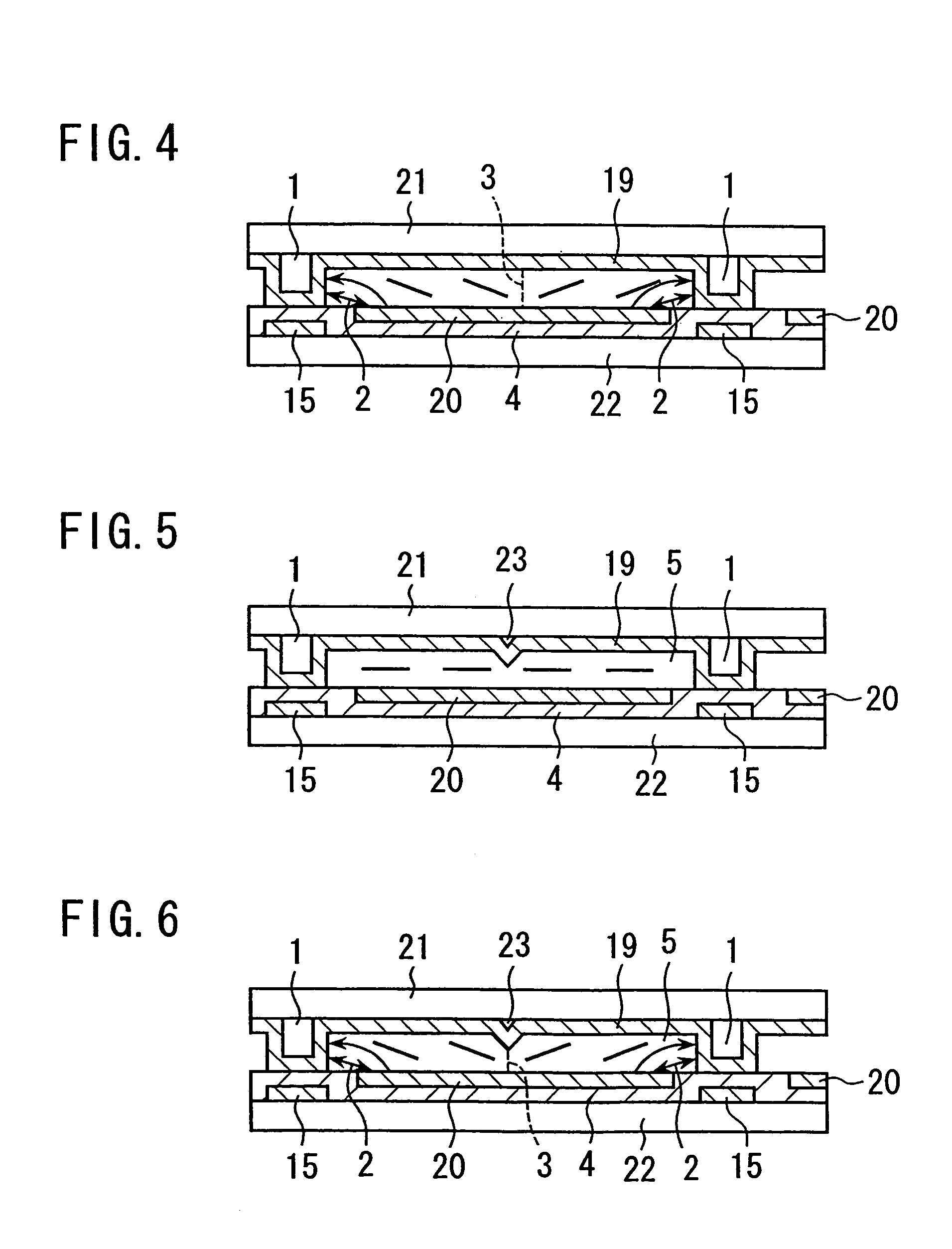
[0246]FIG. 3 illustrates a schematic cross section of a portion including approximately one pixel of a liquid crystal display element according to the second embodiment.

[0247]Referring to FIG. 3, an explanation will be made on a structure of the liquid crystal display element according to the second embodiment.

[0248]The liquid crystal display element according to the second embodiment comprises a pair of opposing transparent substrates 21 and 22, and liquid crystal material 5 filling the space between the pair of transparent substrates 21 and 22. Here, the pair of opposing transparent substrates 21 and 22 constitute an upper substrate 21 and a lower substrate 22.

[0249]The liquid crystal material 5 can be any of liquid crystal materials mentioned above with reference to the first embodiment. Also, operation mode of the liquid crystal material 5 may be any of the operation modes mentioned above with reference to the first embodiment. Further, this embodiment can also be ...

embodiment 3

[Embodiment 3]

[0259]An explanation will be made on a liquid crystal display element according to the third embodiment.

[0260]The liquid crystal display element according to the third embodiment has substantially the same structure as that of the liquid crystal display element according to the second embodiment, except for the following.

[0261]That is, in the liquid crystal display element according to the third embodiment, an optical treatment such as UV treatment and the like is performed on at least one of the upper substrate 21 and the lower substrate 22. By such optical treatment, it is possible to produce aligning force to obtain domains having different alignments of liquid crystal molecules 5 at the interface between the liquid crystal material and the substrate or substrates on which the optical treatment is performed. Also, the pretilt angle of the liquid crystal molecules 5 can be any value. Further, similarly to the second embodiment, the width of the portion where the tran...


PUM

PropertyMeasurementUnit
bearing angleaaaaaaaaaa
pretilt angleaaaaaaaaaa
widthaaaaaaaaaa

Abstract

A liquid crystal display having a wide viewing angle and easily manufactured. The liquid crystal display comprises an upper substrate and a lower substrate, and a liquid crystal material disposed between the upper substrate and the lower substrate. The liquid crystal display has a conductive protrusion disposed on the surface of the upper substrate opposing to the lower substrate. The conductive protrusion is disposed over a scanning electrode line or a signal electrode line and has the same potential as that of the upper electrode. As another structure, each of pixel electrodes on the lower substrate has a smaller area than that of a common electrode on the upper substrate and is covered by the common electrode, and each of the pixel electrodes comprises an electrode portion having approximately symmetrical shape.

Description

[0001]This application is a division of U.S. patent application Ser. No. 10 / 252,982, filed Sep. 23, 2002, now U.S. Pat. No. 6,812,986 which is a division of Ser. No. 09 / 593,119, filed Jun. 13, 2000, now U.S. Pat. No. 6,504,592, which claims the benefit of priority from Japanese Patent Application No. 16-9753 / 1999, filed Jun. 16, 1999, Japanese Patent Application No. 17-3004 / 1999, filed Jun. 18, 1999, and Japanese Patent Application No. 00-3435 / 2000 filed Jan. 12, 2000.FIELD OF THE INVENTION[0002]The present invention relates generally to a liquid crystal display, a method of manufacturing the liquid crystal display and a method of driving the liquid crystal display. More particularly, the present invention relates to a liquid crystal display which has a wide viewing angle, in which disturbance of alignment of liquid crystal molecules can be reduced and which is easily manufactured.BACKGROUND OF THE INVENTION[0003]Liquid crystal displays have been increasingly becoming popular as dis...

Claims


Application Information

Patent Timeline
Patent Type & Authority Patents(United States)
IPC IPC(8): G02F1/1343G02F1/1333G02F1/1339
CPCG02F1/133707G02F1/13394G02F1/134336G02F2001/13373G02F2001/136218G02F2201/121G02F2201/122G02F1/13373G02F1/136218
Inventor TAKATORI, KEN-ICHISUZUKI, MASAYOSHIISHII, TOSHIYASUZUKI, TERUAKIKANOH, HIROSHISUMIYOSHI, KENSAKAMOTO, MICHIAKIOKAMOTO, MAMORUYAMAMOTO, YUJIMATSUYAMA, HIROAKIKAWADA, KIYOMISUZUKI, SEIJIHIRAI, YOSHIHIKO
Owner GOLD CHARM LTD
Why Eureka
Try Eureka