Plating seed layer including an oxygen/nitrogen transition region for barrier enhancement

a technology of oxygen/nitrogen transition region and plating seed, which is applied in the direction of semiconductor devices, semiconductor/solid-state device details, electrical apparatus, etc., can solve the problems of poor ru and ir metal diffusion barrier, conformality and coverage issues of pvd-based deposition techniques, reliability concerns and yield degradation, etc., to enhance the diffusion barrier resistance of the plating seed, enhance the interconnect metal diffusion enhancement, and enhance the conductive material

Inactive Publication Date: 2007-05-08
GLOBALFOUNDRIES INC
View PDF7 Cites 5 Cited by
  • Summary
  • Abstract
  • Description
  • Claims
  • Application Information

AI Technical Summary

Benefits of technology

[0007]In view of the problems mentioned herein above, the present application provides an interconnect structure which includes a plating seed layer that has enhanced conductive material, preferably, Cu, diffusion properties thus eliminating the need for utilizing separate diffusion and seed layers. Specifically, the present invention provides an oxygen / nitrogen transition region within a plating seed layer for interconnect metal diffusion enhancement. The plating seed layer may include Ru, Ir or alloys thereof, and the interconnect conductive material may include Cu, Al, AlCu, W, Ag, Au and the like. Preferably, the interconnect conductive material is Cu or AlCu. In more specific terms, the present invention provides a single seeding layer which includes an oxygen / nitrogen transition region sandwiched between top and bottom seed regions. The presence of the oxygen / nitrogen transition region within the plating seed layer dramatically enhances the diffusion barrier resistance of the plating seed. It is noted that the inventive plating seed layer including the oxygen / nitrogen transition region sandwiched between bottom and top plating seed regions is an improvement over the prior art since a single plating seed layer can be used that has enhanced diffusion properties, yet is capable of serving as a plating seed layer. In the prior art, two separate layers including a diffusion barrier comprised of TaN, for example, and a metallic seed layer are used.

Problems solved by technology

However, with decreasing critical dimension, it is expected that the PVD-based deposition techniques will run into conformality and coverage issues.
These, in turn, will lead to fill issues at plating, such as center and edge voids, which cause reliability concerns and yield degradation.
However, Ru and Ir are not a good metal diffusion barrier as compared with TaN, and, as such, it would be necessary to enhance the barrier resistant of the plating seed.
To date, there is no known prior art that provides an interconnect structure which includes a single Ru or Ir seed layer that has enhanced barrier properties, i.e., resistant to diffusion of an interconnect conductive material such as, for example, Cu, Al, AlCu, W, Ag, and Au.

Method used


Image

  • Plating seed layer including an oxygen/nitrogen transition region for barrier enhancement
  • Plating seed layer including an oxygen/nitrogen transition region for barrier enhancement
  • Plating seed layer including an oxygen/nitrogen transition region for barrier enhancement

Examples


Embodiment Construction

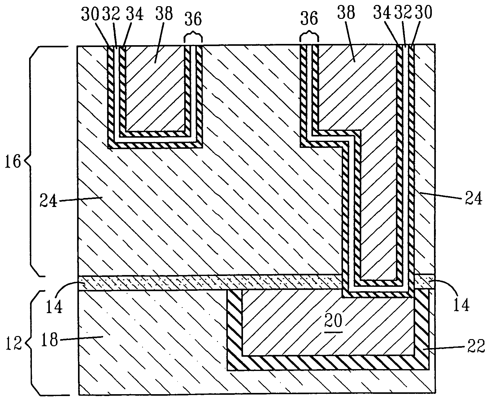
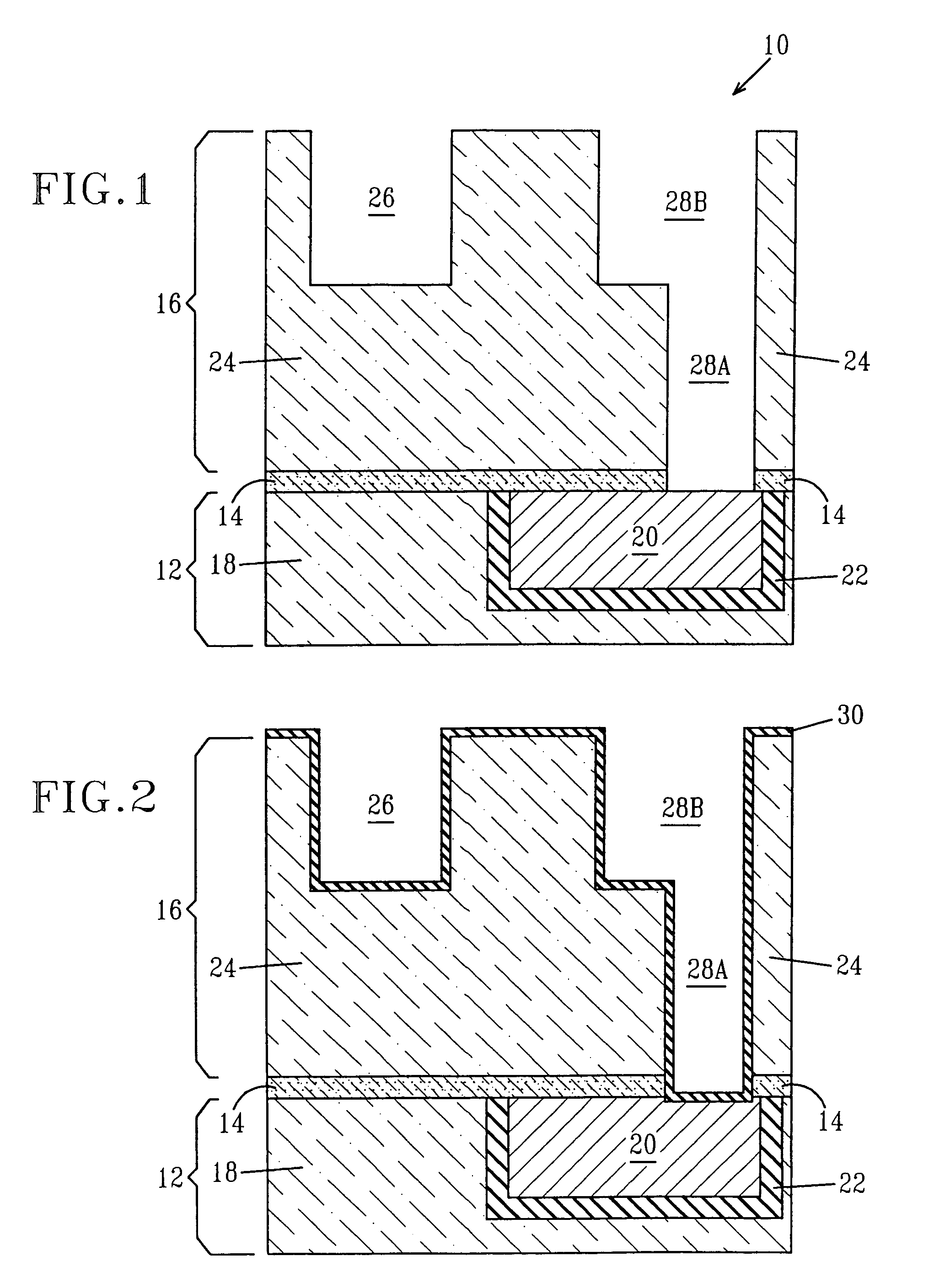
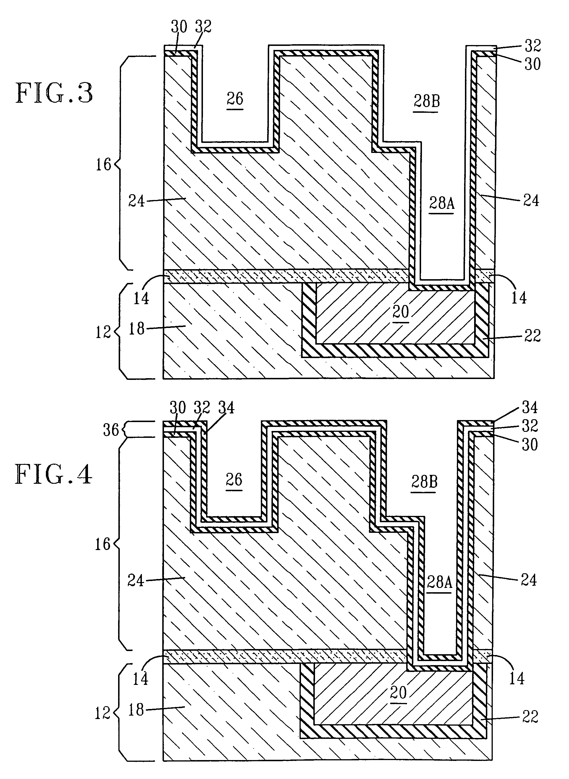
[0025]The present invention, which provides an interconnect structure including a single plating seed layer having enhanced resistant to metal diffusion and a method of fabricating the same, will now be described in greater detail by referring to the following discussion and drawings that accompany the present application. The drawings of the present application, which are referred to herein below in greater detail, are provided for illustrative purposes and, as such, they are not drawn to scale.

[0026]The process flow of the present invention begins with providing the initial interconnect structure 10 shown in FIG. 1. Specifically, the initial interconnect structure 10 shown in FIG. 1 comprises a multilevel interconnect including a lower interconnect level 12 and an upper interconnect level 16 that are separated in part by dielectric capping layer 14. The lower interconnect level 12, which may be located above a semiconductor substrate including one or more semiconductor devices, co...


PUM


Abstract

An interconnect structure which includes a plating seed layer that has enhanced conductive material, preferably, Cu, diffusion properties is provided that eliminates the need for utilizing separate diffusion and seed layers. Specifically, the present invention provides an oxygen / nitrogen transition region within a plating seed layer for interconnect metal diffusion enhancement. The plating seed layer may include Ru, Ir or alloys thereof, and the interconnect conductive material may include Cu, Al, AlCu, W, Ag, Au and the like. Preferably, the interconnect conductive material is Cu or AlCu. In more specific terms, the present invention provides a single seeding layer which includes an oxygen / nitrogen transition region sandwiched between top and bottom seed regions. The presence of the oxygen / nitrogen transition region within the plating seed layer dramatically enhances the diffusion barrier resistance of the plating seed.

Description

FIELD OF THE INVENTION[0001]The present invention relates to a semiconductor structure and a method of fabricating the same. More particularly, the present invention relates to an interconnect structure which includes a plating seed layer that comprises an oxygen / nitrogen transition region located between first and second plating regions. The plating seed layer of the present invention, which includes the oxygen / nitrogen transition region, dramatically increases the diffusion barrier resistance of the plating seed layer compared with prior art plating seed layers that do not include the oxygen / nitrogen transition region. The present invention also provides a method of fabricating such an interconnect structure.BACKGROUND OF THE INVENTION[0002]Generally, semiconductor devices include a plurality of circuits which form an integrated circuit fabricated on a semiconductor substrate. A complex network of signal paths will normally be routed to connect the circuit elements distributed on ...

Claims


Application Information

Patent Timeline
Patent Type & Authority Patents(United States)
IPC IPC(8): H01L23/58
CPCH01L21/76843H01L21/76844H01L21/76846H01L21/76856H01L21/76873H01L23/53238H01L2924/0002H01L2221/1089H01L2924/00H01L21/28
Inventor YANG, CHIH-CHAOGAUDET, SIMONLAVOIE, CHRISTIANPONOTH, SHOMSPOONER, TERRY A.
Owner GLOBALFOUNDRIES INC
Why Eureka
Try Eureka