Electrophoretic display and methods of addressing such display

a technology of electrophoretic displays and backplanes, applied in the field of electrophoretic displays and methods of addressing such displays, can solve the problems of mechanism failure, low cost, high resolution backplanes that cannot be driven commercially, etc., and achieve the effect of significant speed enhancemen

Active Publication Date: 2008-08-05
E INK CORPORATION
View PDF10 Cites 139 Cited by
  • Summary
  • Abstract
  • Description
  • Claims
  • Application Information

AI Technical Summary

Benefits of technology

[0010]The objective of the present invention is to provide low cost display devices and driving methods for addressing such displays.
[0014]In the writing / drawing process, an electrical field is created between the conductive surface or tip of the movable element (on the dielectric layer side of the electrophoretic display panel) and the stationary electrode layer (on the opposite side of the electropheretic display panel), with the highest field intensity located at the contact point of the movable element. As the movable element moves across the surface of the dielectric barrier layer, the peak of the electric field moves with it. When the strength of the electric field across electrophoretic display panel between the contact point of the movable element and the stationary electrode is sufficient, the charged pigment particles would move, according to the polarity of the applied electric field, to form an image. Therefore as the movable element moves, images are formed due to the movement of the charged pigment particles under the influence of the electric field. Therefore the movement of the movable element provides the perception that images are being written / drawn on the electrophoretic display panel.
[0016]Many non-conductive liquids are good dielectric materials with strong polarization ability in an electric field that can minimize the impact of adding an extra liquid layer to the multi-layer display panel between the conductive surface or tip of the movable element and the stationary electrode layer. The portion of the electrical field strength allocated to the added liquid layer is negligible compared to the electric field strength experienced by the electrophoretic fluid. Depending on the properties of the non-conductive liquid used, the total electric field needed to address an electrophoretic display panel with a movable element having at least a conductive surface or tip can be reduced drastically. The selection criterion for the non-conductive liquid is that the non-conductive liquid should not cause swelling or permeation through the dielectric layer.
[0017]The other advantage of the use of a non-conductive liquid between the movable element and the dielectric barrier layer of the electrophoretic display panel is to ease the mechanical strength requirement of the display panel. It eliminates the need of contact pressure between the movable element and the dielectric barrier layer of the display panel. It also reduces the requirement on surface smoothness of the movable element and abrasion resistance of the dielectric barrier layer.
[0018]Other advantages of this invention include the resolution of the image controlled by the size of the liquid path which can be very small.
[0021]A movable element in the form of a roller or the like may move to be in contact with the non-conductive liquid droplets to drive the charged pigment particle at the contact point. The dispensing speed of the movable element may exceed the moving speed of the charged pigment particles, thus providing significant writing speed enhancement.

Problems solved by technology

However, currently there are no commercially available low cost high resolution backplanes for driving large size electrophoretic displays.
In addition, both direct drive with a dot matrix patterned electrode and active matrix drive with a TFT backplane need driving electronics that are too expensive for large size displays.
The mechanism worked well in theory, but ran into difficulty in practical applications.
The main obstacle is the poor electrical contact between the movable electrode and the surface of the electrophoretic display panel.
When the movable electrode is in contact with the surface of the electrophoretic display panel, due to rigidity and surface roughness of both the movable electrode tip and the electrophoretic display panel, the interface is dominated by air pockets and as a result, there is very limited true contact area.
The poor contact results in a significant loss of electric field intensity at the contact interface and diminishes the electric field intensity across the electrophoretic display panel.
However, in these methods, the resolution of the image is inevitably limited by the resolution of either the printed circuit board or the pre-deposited conductive pads.

Method used


Image

  • Electrophoretic display and methods of addressing such display
  • Electrophoretic display and methods of addressing such display
  • Electrophoretic display and methods of addressing such display

Examples


Embodiment Construction

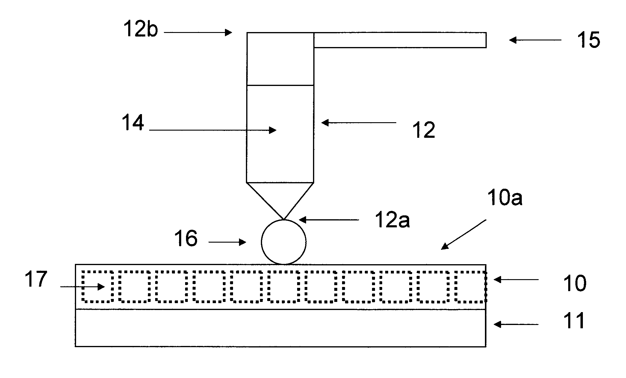
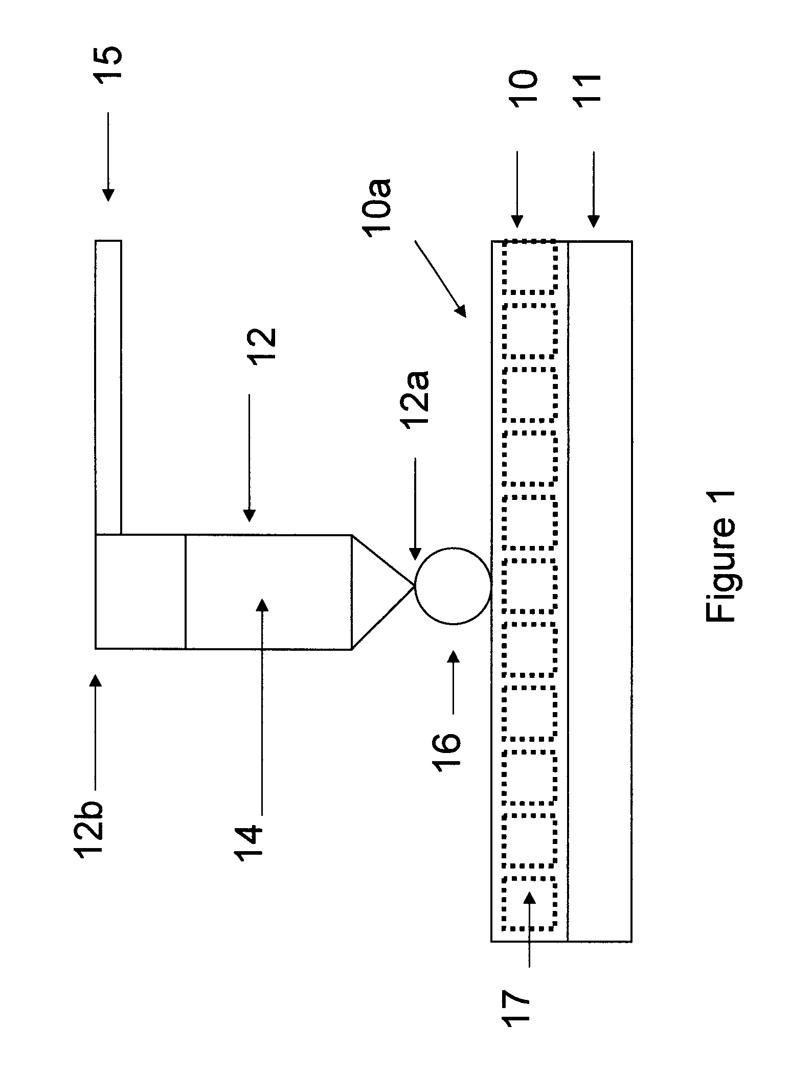
[0023]FIG. 1 illustrates an electrophoretic display of the present invention which comprises a stationary electrode layer (11), an electrophoretic display panel (10) comprising display cells (17), a movable element (12) having a conductive tip and a non-conductive liquid (14) filled in the body of the movable element. One side of the display panel has a dielectric surface (10a). The liquid released from the movable element in the form of droplets causes contact between the electrophoretic display panel (10) and the conductive tip of the movable element (12) which in turn forms a temporary yet an integrated electrical field between the stationary electrode layer (11) and the conductive tip of the movable element (12). The movable element comprises two parts 12a and 12b. The part, 12a, as stated, is conductive and is connected to a voltage source (not shown). The other part, 12b, may be linked to a robotic arm (15) which controls the movement of the movable element

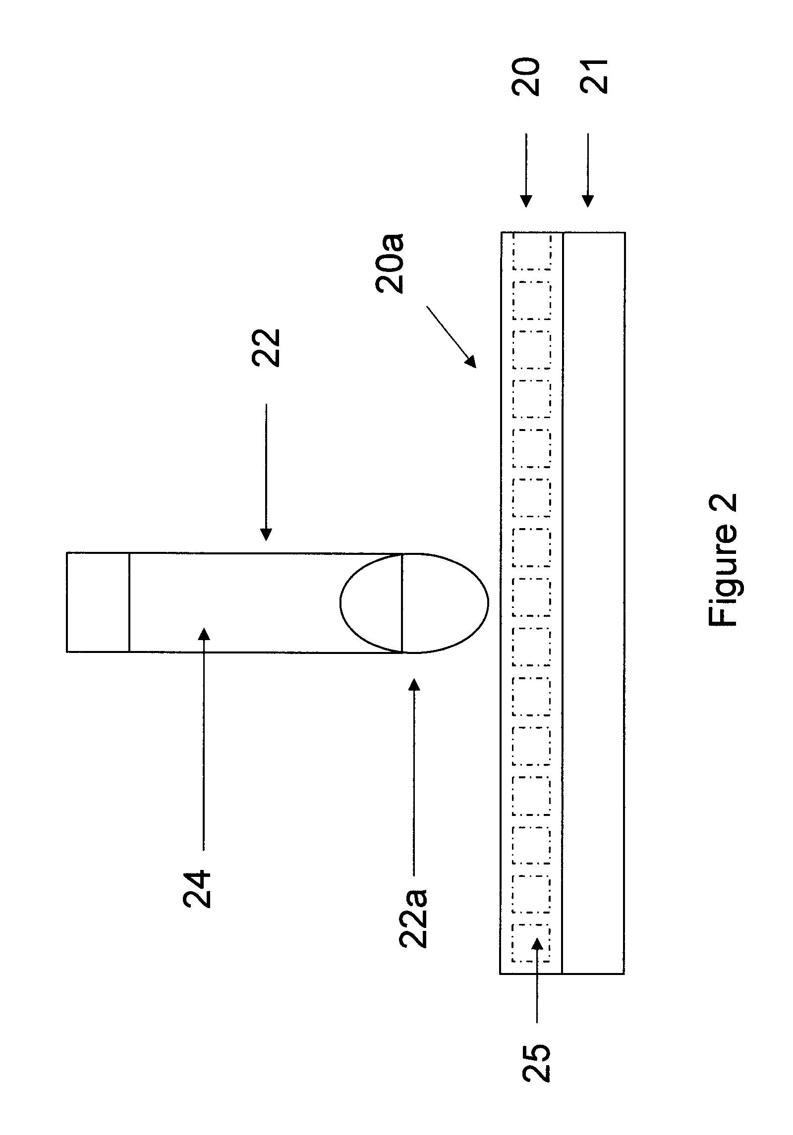
[0024]FIG. 2 illustr...


PUM


Abstract

The present invention relates to electrophoretic displays and methods of addressing such displays. The displays and methods are especially suitable for large size electronic boards or signs.

Description

[0001]The present application claims the benefit of U.S. Provisional Application 60 / 721,859, filed Sep. 28, 2005; the contents of which are incorporated herein by reference in its entirety.FIELD OF THE INVENTION[0002]The present invention relates to electrophoretic displays and methods of addressing such displays. The displays and methods are especially suitable for large size electronic boards or signs.BACKGROUND OF THE INVENTION[0003]The electrophoretic display (EPD) is a non-emissive device based on the electrophoresis phenomenon influencing the migration of charged pigment particles in a solvent, preferably a colored dielectric solvent. This type of display was first proposed in 1969. An electrophoretic display typically comprises a pair of opposed, spaced-apart plate-like electrodes, with spacers predetermining a certain distance between them. At least one of the electrodes, typically on the viewing side, is transparent. For the passive type of electrophoretic displays, row and...

Claims


Application Information

Patent Timeline
Patent Type & Authority Patents(United States)
IPC IPC(8): G02B26/00G06F3/041G09G3/34G02F1/167G02F1/1676
CPCG02F1/167G02F2001/1676G02F1/1676
Inventor WANG, XIAOJIAMORRIS, DAVIDWANG, FEIHO, ANDREW
Owner E INK CORPORATION
Why Eureka
Try Eureka