Method for reducing SRAM test time by applying power-up state knowledge

a power-up state and knowledge technology, applied in the field of memory testing, can solve the problems of limiting the usable feature size, affecting the performance of the memory, so as to reduce the testing time and mitigate the effect of subsequent testing tim

Active Publication Date: 2007-05-08
TEXAS INSTR INC
View PDF5 Cites 22 Cited by
  • Summary
  • Abstract
  • Description
  • Claims
  • Application Information

AI Technical Summary

Benefits of technology

[0012]In one aspect of the present invention the method comprises powering-up the memory device and reading a preferred (or intrinsic) power-up data state of each cell of the memory device without memory initialization or writes. The method then captures and stores the data state of each cell and utilizes the stored power-up data states or an inverse of the power-up data states to tailor a test pattern used by the test algorithm for further memory testing. Thus, additional reading of the memory cell in the preferred data state is unnecessary, permitting reduced testing times, particularly in the case of data retention and cell disturb testing times.
[0013]In another aspect of the present invention, the test pattern data (e.g., 0 and 1 data, a checkerboard test, or a characterization pattern) used in various conventional testing algorithms of an SRAM device (e.g., a 6T SRAM) may be replaced by the stored power-up data states or an inverse of the power-up data states. In this way prior knowledge of the individual bit behavior at power-up is preserved to mitigate subsequent testing time.

Problems solved by technology

Memory test algorithms are written to uncover faults with storage cells and the access to these storage cells arising from improper design, lack of design margins or processing deficiencies.
Generally, these algorithms are written to be extensive and exhaustive to ensure that no bit defects, either hard defects or intermittent failures find their way into the field.
As semiconductor features are aggressively reduced, for example, local mismatches between SRAM transistors have increased; presenting greater problems that may limit the usable feature size.
Additionally, small misalignments between any two layers (e.g., moat and gate) have resulted in larger mismatches for more advanced technology nodes.
For example, in situations where there is misalignment, a right transistor Vt may be altered more or less than a left transistor Vt, thereby disadvantageously creating transistor mismatch.
Since a plurality of transistors are utilized in SRAM requiring matched electrical characteristics, and since the negative effects of matching may become more prevalent as transistor widths are reduced, transistor mismatching issues may present themselves to a great degree in SRAM, particularly as that type of memory is continually scaled down.

Method used


Image

  • Method for reducing SRAM test time by applying power-up state knowledge
  • Method for reducing SRAM test time by applying power-up state knowledge
  • Method for reducing SRAM test time by applying power-up state knowledge

Examples


Embodiment Construction

[0021]One or more aspects of the present invention are described with reference to the drawings, wherein like reference numerals are generally utilized to refer to like elements throughout, and wherein the various structures are not necessarily drawn to scale. In the following description, for purposes of explanation, numerous specific details are set forth in order to provide a thorough understanding of one or more aspects of the present invention. It may be evident, however, to one skilled in the art that one or more aspects of the present invention may be practiced with a lesser degree of these specific details. In other instances, known structures and devices are shown in block diagram form in order to facilitate describing one or more aspects of the present invention.

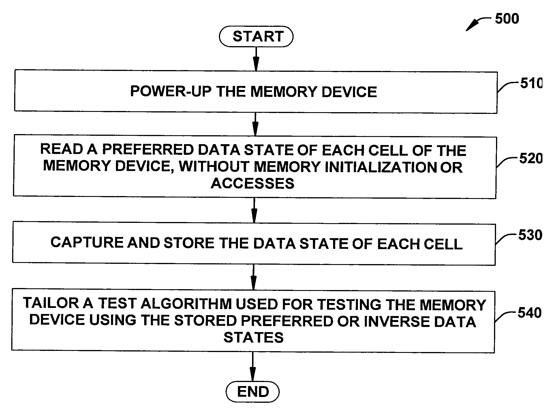
[0022]The present invention pertains to a method of tailoring a test algorithm used in the testing of SRAM memory devices utilizing the preferred power-up data state of each memory cell.

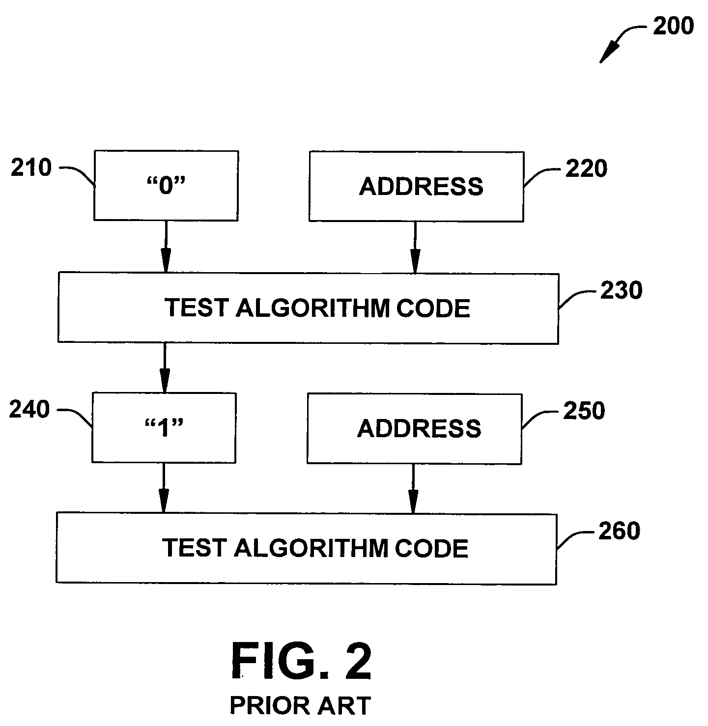
[0023]Conventional test algo...


PUM


Abstract

Methods (400, 500, and 600) are disclosed for testing a memory device by tailoring an algorithm (460) used in the testing based on the preferred or intrinsic data state 425 that is obtained upon power-up of an advanced technology SRAM memory device (100). The methods (400, 500, and 600) take advantage of the observation that such SRAM devices repeatedly power-up in a preferred state 310. Accordingly, one method 500 comprises powering-up 510 the memory device and reading 520 a preferred power-up data state of each cell of the memory device without memory initialization or writes. The method 500 then captures and stores 530 a data state associated with the preferred power-up data state of each cell 100 and utilizes the stored power-up data state 310 or an inverse of the power-up data state 320 to tailor 540 a test pattern used by the test algorithm 460.

Description

FIELD OF INVENTION[0001]The present invention relates generally to semiconductor processing, and more particularly to testing a memory in a manner that reduces testing time, particularly when utilized in static random access memory (SRAM).BACKGROUND OF THE INVENTION[0002]Memory test algorithms are written to uncover faults with storage cells and the access to these storage cells arising from improper design, lack of design margins or processing deficiencies. Generally, these algorithms are written to be extensive and exhaustive to ensure that no bit defects, either hard defects or intermittent failures find their way into the field. As such, in addition to straight forward writing and reading from storage cells, various methods of disturbing the bits have been devised and employed. Some algorithms write and read at one voltage and read and write at another voltage to check for slew margins.[0003]Data retention tests are also being performed with more frequency lately as memory cells...

Claims


Application Information

Patent Timeline
Patent Type & Authority Patents(United States)
IPC IPC(8): G11C29/00
CPCG11C29/10G11C29/36G11C11/41G11C2029/0407
Inventor LOH, WAH KIT
Owner TEXAS INSTR INC
Why Eureka
Try Eureka