Leadframe designs for integrated circuit plastic packages

a technology of plastic packaging and integrated circuits, which is applied in the direction of semiconductor devices, semiconductor/solid-state device details, electrical apparatus, etc., can solve the problems of limited effect of comparatively low electrical conductivity of steel, high cost of packaging, and significant reduction of thermal conductivity of steel compared with copper

Active Publication Date: 2007-05-22
BELL SEMICON LLC
View PDF3 Cites 10 Cited by
  • Summary
  • Abstract
  • Description
  • Claims
  • Application Information

AI Technical Summary

Benefits of technology

[0008]A new leadframe design for high power transistor packages has been developed in which the leadframe body is formed of a composite of materials. This allows the portions of the leadframe that require strength to be formed of a high strength material, e.g. steel, while the paddle portion of the leadframe is formed of a high thermal conductivity material, e.g. copper. The copper paddle portion serves as an effective heat sink for the power transistor. This composite leadframe optimizes thermal and mechanical performance at low cost. In the preferred embodiment the leadframe is steel and is provided with a center cutout, where the die is attached. A copper insert is assembled in the cutout. The copper insert provides an effective heat sink, while the remainder of the leadframe provides the desired mechanical strength. The invention is aimed at plastic cavity packages but may be used in conventional overmolded plastic packages.

Problems solved by technology

These packages are expensive.
It is recognized that the comparatively low electrical conductivity of steel is of limited consequence in a leadframe where the paddle is not a conductor member.
However, the lower thermal conductivity of steel compared with copper is significant in a power transistor device.
A major issue in the design and performance of power transistors is heat dissipation.
The steel paddle may not afford an effective heat sink for some power transistors.

Method used


Image

  • Leadframe designs for integrated circuit plastic packages
  • Leadframe designs for integrated circuit plastic packages
  • Leadframe designs for integrated circuit plastic packages

Examples


Embodiment Construction

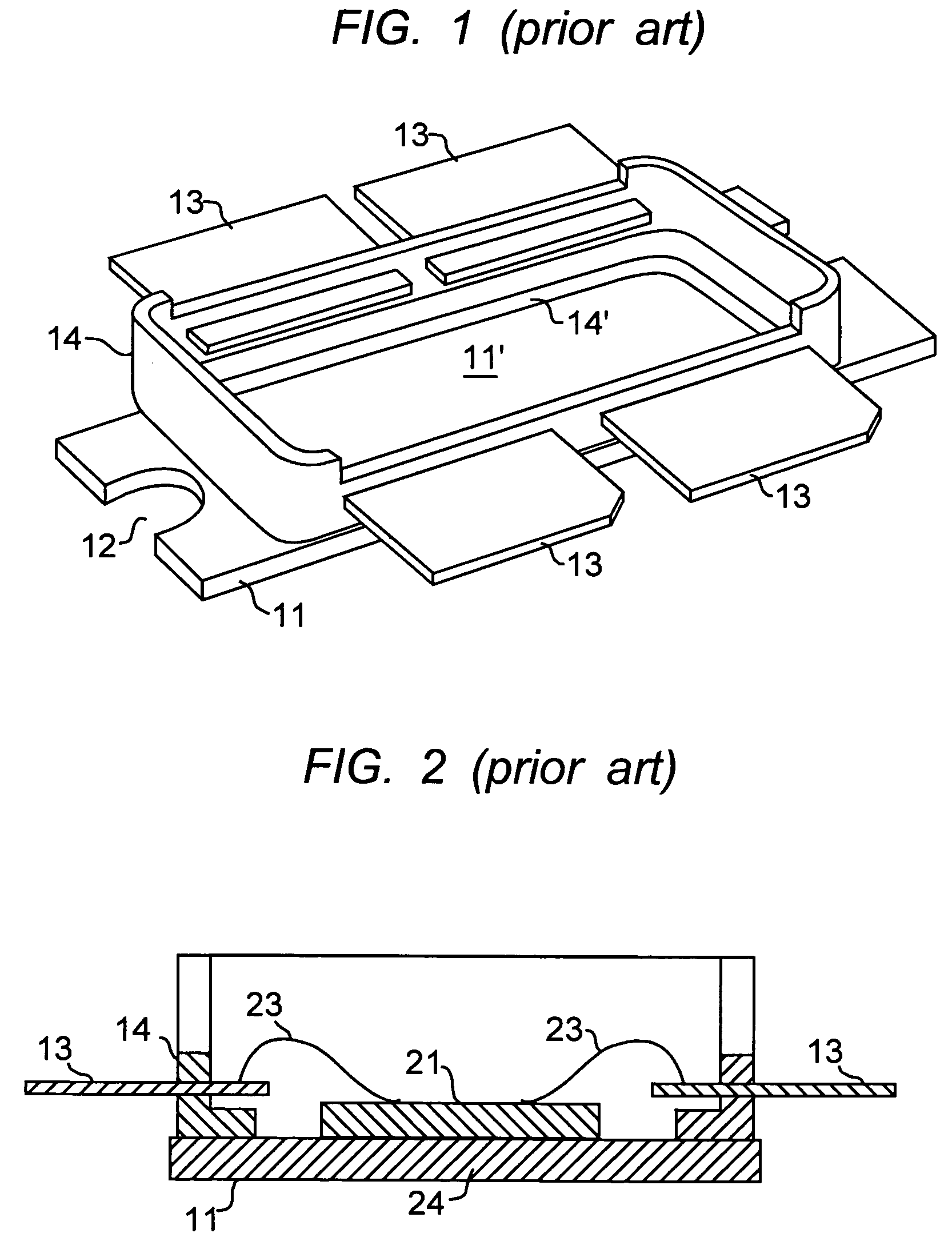
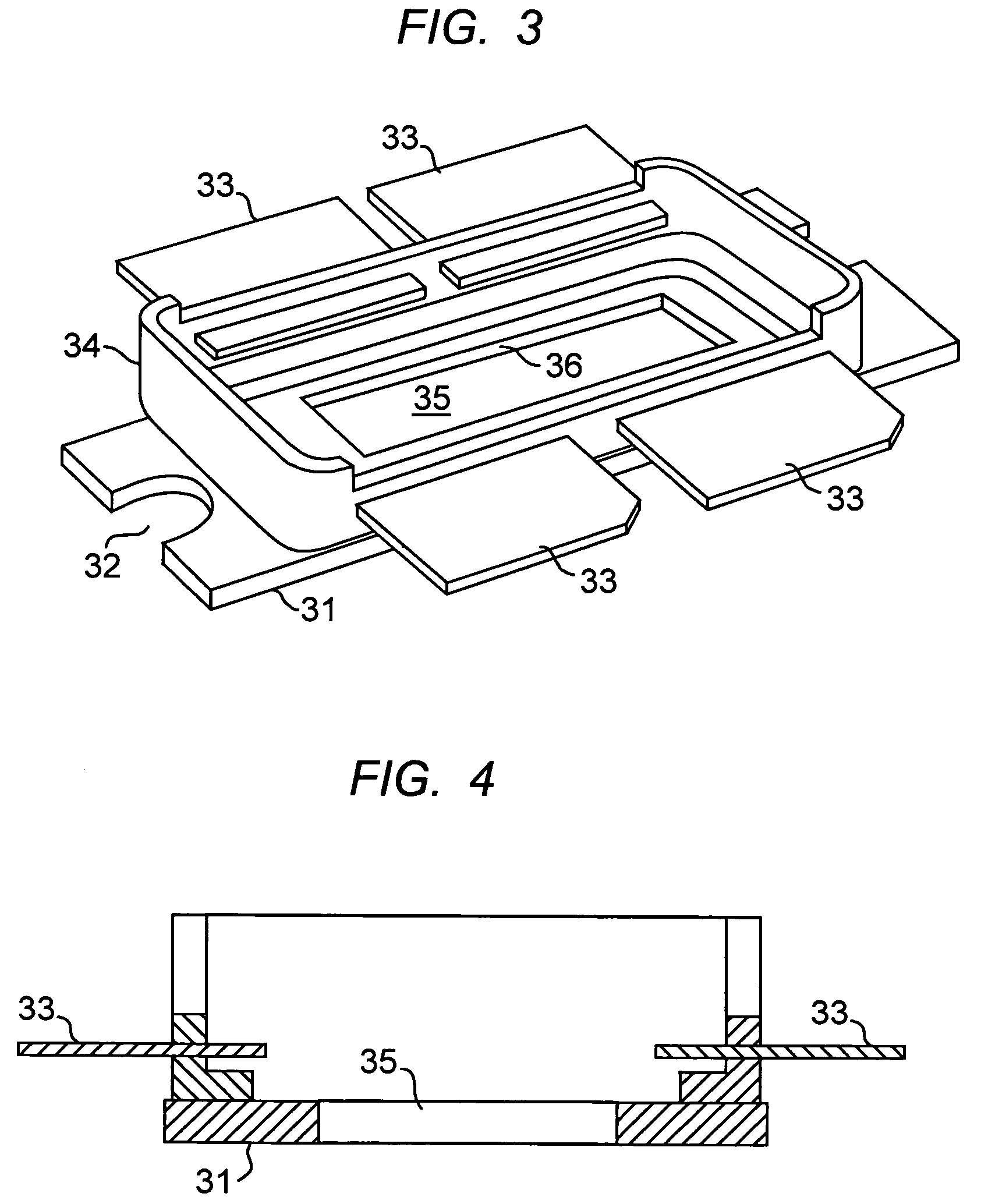
[0017]The invention will be described in more detail using, as a prototypical package, a plastic cavity RFLDMOS power transistor package. The invention was developed around this type of package and it represents a preferred embodiment. However, it should be understood that other kinds of IC devices may be packaged using the approach described. Also other types of IC packages may favorably utilize the essential features of the invention. The plastic cavity packaging format is represented here by way of example only. A wide variety of plastic package designs are available in the packaging industry, including plastic overmolded packages. Many will share the properties described below. All plastic package products that have the features to be described are intended to be included in the scope of the invention.

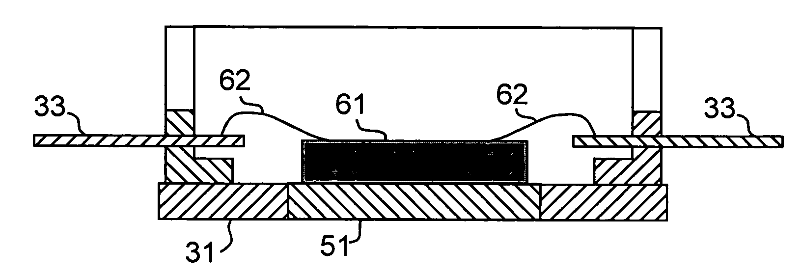
[0018]Referring to FIG. 1, a perspective view of a plastic cavity package is shown with a metal chip support member 11 comprising at least a portion of what is conventionally consi...


PUM


Abstract

The specification describes a plastic cavity package design for high power transistor packages in which the leadframe is formed of a composite of materials. This allows the portions of the leadframe that require strength to be formed of a high strength material, e.g. steel, while the paddle portion of the leadframe is formed of a high thermal conductivity material, e.g. copper. This composite leadframe optimizes thermal and mechanical performance at low cost. In the preferred embodiment the leadframe is provided with a center cutout, where the die is attached. A copper insert is assembled in the cutout. The copper insert provides an effective heat sink, while the remainder of the leadframe provides the desired mechanical strength.

Description

FIELD OF THE INVENTION[0001]This invention relates to leadframe designs used in plastic overmolded packages for integrated circuit (IC) and related devices.BACKGROUND OF THE INVENTION[0002](Portions of the technical material contained in this section may not be prior art.)[0003]A common element in packaging electronic IC devices is a plastic housing. In the most typical IC plastic package, electronic components are assembled on a metal leadframe and a polymer is molded over the assembly to encapsulate the device and portions of the leadframe. The leadframe serves not only to support the electronic components, but has metal tabs that extend from the overmolded plastic and provide a means to electrically connect to the encapsulated electronic components.[0004]Recent modifications of the molded plastic IC package include an air cavity design wherein the housing for the package is plastic, but is pre-molded over a lead frame before the IC device is assembled into the package. This desig...

Claims


Application Information

Patent Timeline
Patent Type & Authority Patents(United States)
IPC IPC(8): H01L23/495H01L23/10
CPCH01L23/047H01L23/24H01L23/49861H01L23/293H01L2224/48091H01L2224/48247H01L2924/01079H01L2924/00014H01L24/48H01L2924/10253H01L2924/15747H01L2924/00H01L2924/14H01L2224/45099H01L2224/45015H01L2924/207
Inventor BAMBRIDGE, TIMOTHY B.
Owner BELL SEMICON LLC
Why Eureka
Try Eureka