Photoelectric conversion apparatus which avoids certain shading effects

a conversion apparatus and photoelectric technology, applied in the field of photoelectric conversion apparatus, can solve the problems of deteriorating image quality, affecting the quality of photoelectric conversion, and affecting the quality of photoelectric conversion, and achieve the effect of high-quality photoelectric conversion

Inactive Publication Date: 2007-05-22
CANON KK
View PDF18 Cites 35 Cited by
  • Summary
  • Abstract
  • Description
  • Claims
  • Application Information

AI Technical Summary

Benefits of technology

[0019]With the above arrangements, a high-quality

Problems solved by technology

The image quality is greatly deteriorated.
The wirings used in the photoelectric conversion apparatus tend to be thin and long.
Voltage drop by the resistance r1 of the vertical output line 6 poses a serious problem.
Another problem is posed by different dynamic ranges of the source follower circuit i

Method used


Image

  • Photoelectric conversion apparatus which avoids certain shading effects
  • Photoelectric conversion apparatus which avoids certain shading effects
  • Photoelectric conversion apparatus which avoids certain shading effects

Examples


first embodiment

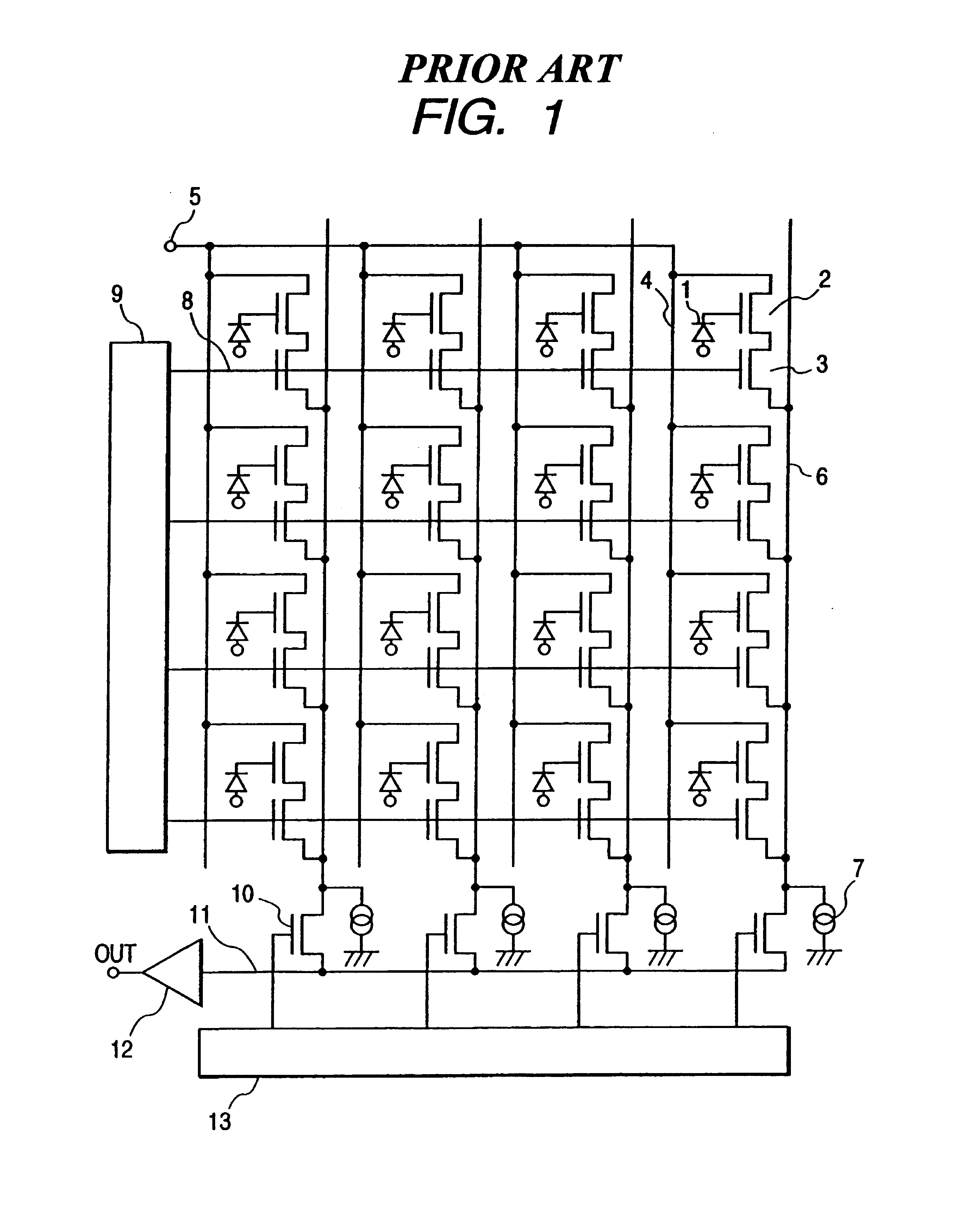
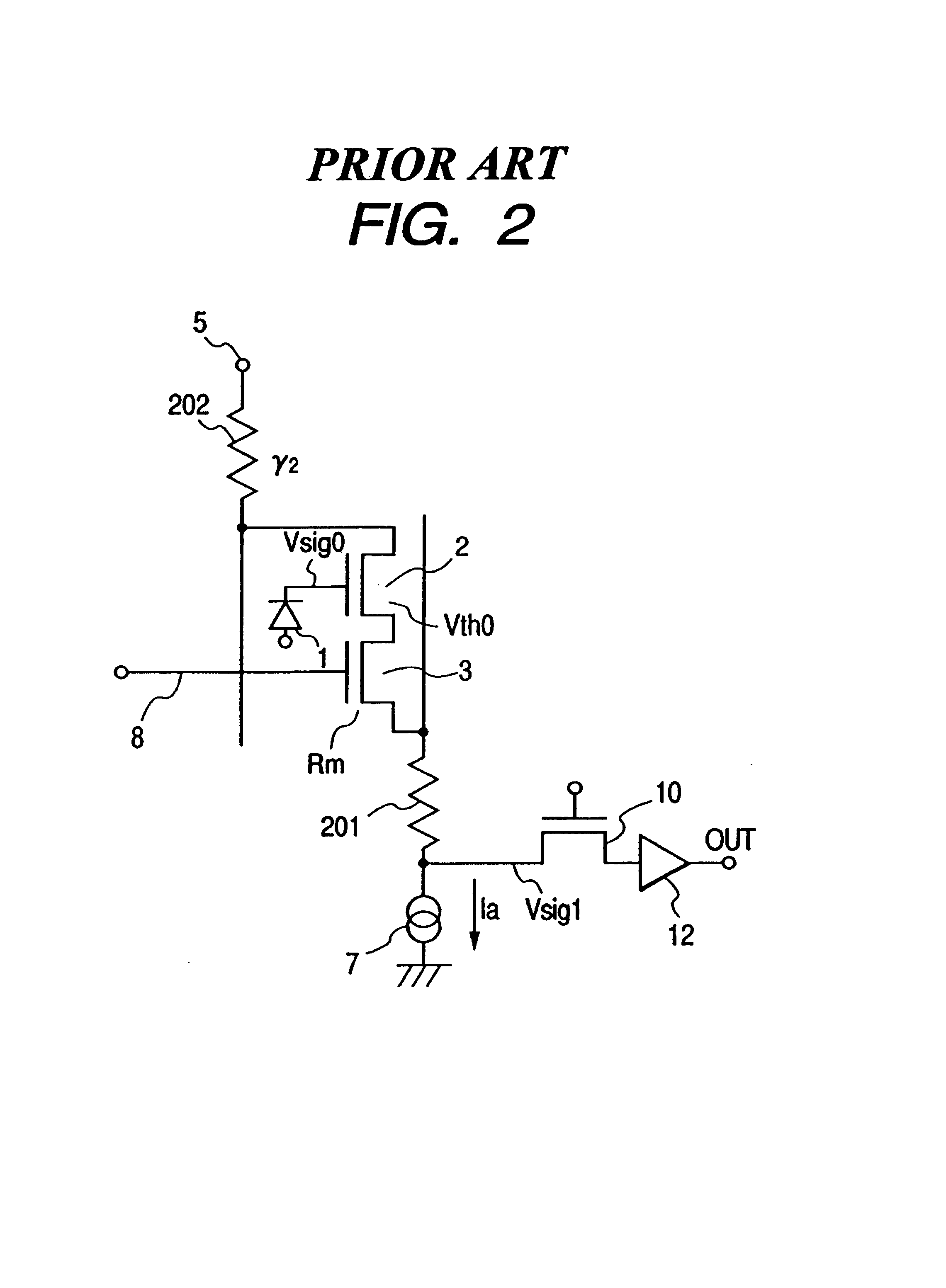
[0029]FIG. 3 is a diagram for explaining the present invention. Constant current sources 7 are located on the side vertically opposite to the direction of outputting signal voltages from a source follower circuit. Referring to FIG. 3, photoelectric conversion elements (e.g., photodiodes) 1 store charges in accordance with the amounts of incident light and form a two-dimensional array (4×4 elements in FIG. 3). One terminal of the photoelectric conversion element 1 is connected to the gate of a source follower input MOS 2. The source of the source follower input MOS 2 is connected to the drain of a vertical selection switch MOS 3. The drain of the source follower input MOS 2 is connected to a power supply terminal 5 through a power supply line 4. The source of the vertical selection switch MOS 3 is connected to a load power supply 7 through a vertical output line 6. The source follower input MOS 2, the vertical selection switch MOS 3, and load power supply 7 form a source follower cir...

second embodiment

[0042]FIG. 5 is a chart for explaining the present invention. Constant current sources are located on vertically the same side as a direction of outputting signal voltages from source follower circuits, and at the same time, the signal voltages in units of rows are alternately output in opposite directions.

[0043]Referring to FIG. 5, photoelectric conversion elements (e.g., photodiodes) 1 store charges in accordance with the amounts of incident light and form a two-dimensional array (4×4 elements in FIG. 5). One terminal of the photoelectric conversion element 1 is connected to the gate of a source follower input MOS 2. The source of the source follower input MOS 2 is connected to the drain of a vertical selection switch MOS 3. The drain of the source follower input MOS 2 is connected to a power supply terminal 5 through a power supply line 4. The source of the vertical selection switch MOS 3 is connected to a load power supply 7 through a vertical output line 6. The source follower ...

third embodiment

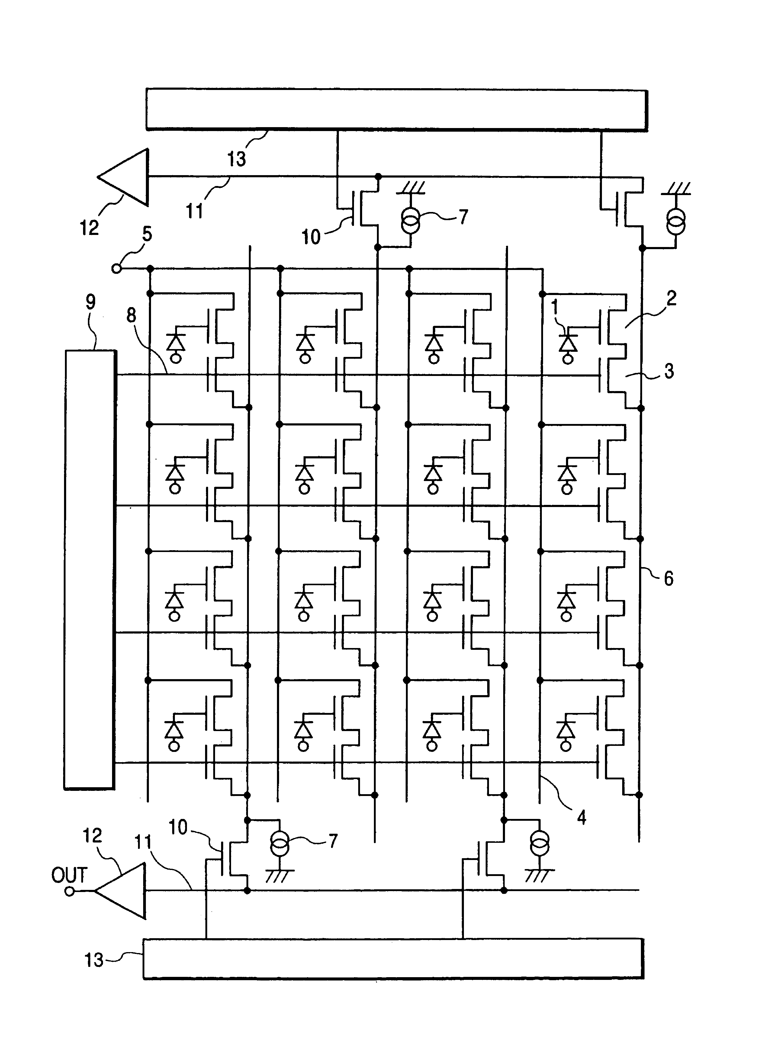
[0056]FIG. 6 is a diagram for explaining the present invention. The power supply terminals of source follower circuits are alternately arranged at vertically opposite positions.

[0057]Referring to FIG. 6, photoelectric conversion elements (e.g., photodiodes) 1 store charges in accordance with the amounts of incident light and form a two-dimensional array (4×4 elements in FIG. 6). One terminal of the photoelectric conversion element 1 is connected to the gate of a source follower input MOS 2. The source of the source follower input MOS 2 is connected to the drain of a vertical selection switch MOS 3. The drain of the source follower input MOS 2 is connected to a power supply terminal 5 through a power supply line 4. The source of the vertical selection switch MOS 3 is connected to a load power supply 7 through a vertical output line 6. The source follower input MOS 2, the vertical selection switch MOS 3, and load power supply 7 form a source follower circuit. The photoelectric convers...


PUM


Abstract

In order to solve the problem in which voltages Vsig1 read in units of rows have differences to cause vertical shading, thereby degrading image quality, and the problem in which the dynamic ranges of source follower circuits are different in units of rows because finite resistances are distributed in the power supply lines, a photoelectric conversion apparatus includes photoelectric conversion portions placed in a plurality of rows, an amplification section including a load section arranged in units of vertical output lines to amplify signal charges accumulated in the photoelectric conversion portions placed in a plurality of rows, a vertical scanning section for sequentially scanning signals amplified by the amplification section to read the signals onto the vertical output lines, and a horizontal scanning section for sequentially scanning the signals amplified by the amplification section to read the signals onto horizontal output lines, wherein the load sections are located on a side vertically opposite to the direction of signal output from the amplification section.

Description

BACKGROUND OF THE INVENTION[0001]1. Field of the Invention[0002]The present invention relates to a photoelectric conversion apparatus having photoelectric conversion elements arrayed in a matrix and being capable of obtaining a high-quality image.[0003]2. Related Background Art[0004]FIG. 1 is a diagram for explaining a conventional photoelectric conversion apparatus. Referring to FIG. 1, photoelectric conversion elements (e.g., photodiodes) 1 store charges in accordance with the amounts of incident light and form a two-dimensional array (4×4 elements in FIG. 1). One terminal of the photoelectric conversion element 1 is connected to the gate of a source follower input MOS 2. The source of the source follower input MOS 2 is connected to the drain of a vertical selection switch MOS 3. The drain of the source follower input MOS 2 is connected to a power supply terminal 5 through a power supply line 4. The source of the vertical selection switch MOS 3 is connected to a load power supply ...

Claims


Application Information

Patent Timeline
IPC IPC(8): H04N3/14H01L31/09H04N5/335H04N5/341H04N5/355H04N5/361H04N5/369H04N5/374H04N5/3745H04N5/378
CPCH04N5/3572H04N5/3658H04N5/3745H04N25/61H04N25/677H04N25/77
Inventor KOCHI, TETSUNOBU
Owner CANON KK
Why Eureka
Try Eureka