

Test structures in unused areas of semiconductor integrated circuits and methods for designing the same
a technology of integrated circuits and test structures, applied in the direction of individual semiconductor device testing, semiconductor/solid-state device testing/measurement, instruments, etc., can solve the problems of increasing the cost of inspections, increasing the complexity of ic's, and unable to hold a very limited number of test structures on the scribe lin
- Summary
- Abstract
- Description
- Claims
- Application Information
AI Technical Summary
Benefits of technology
Problems solved by technology
Method used
Image

Examples
Embodiment Construction
[0024]Reference will now be made in detail to the presently preferred embodiments of the invention, examples of which are illustrated in the accompanying drawings.
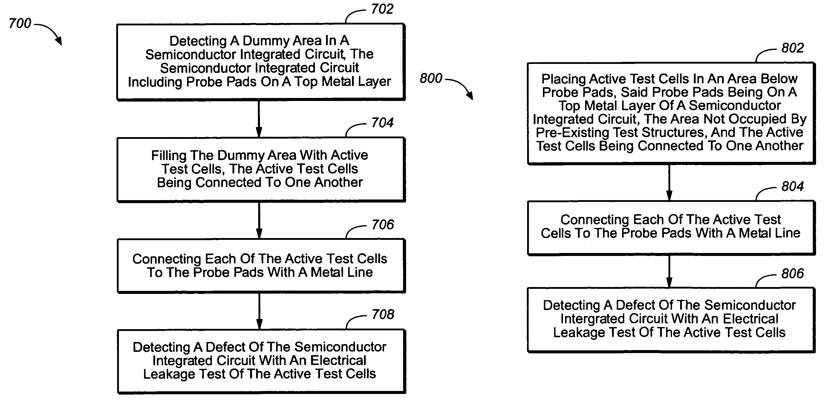
[0025]With the development of deep sub-micron technology, there exists a need to place more test structures in both a test chip and a product chip such as RapidChip™ developed by LSI Logic Corporation, and the like, since previous Q-chip (Qualification-chip) qualification cannot guarantee the later tape-out being successful as well. However, real estate in a semiconductor integrated circuit is precious and limited. Accordingly, the present invention discloses a method and apparatus for placing more test structures in a semiconductor integrated circuit by using unused areas in the semiconductor integrated circuit.
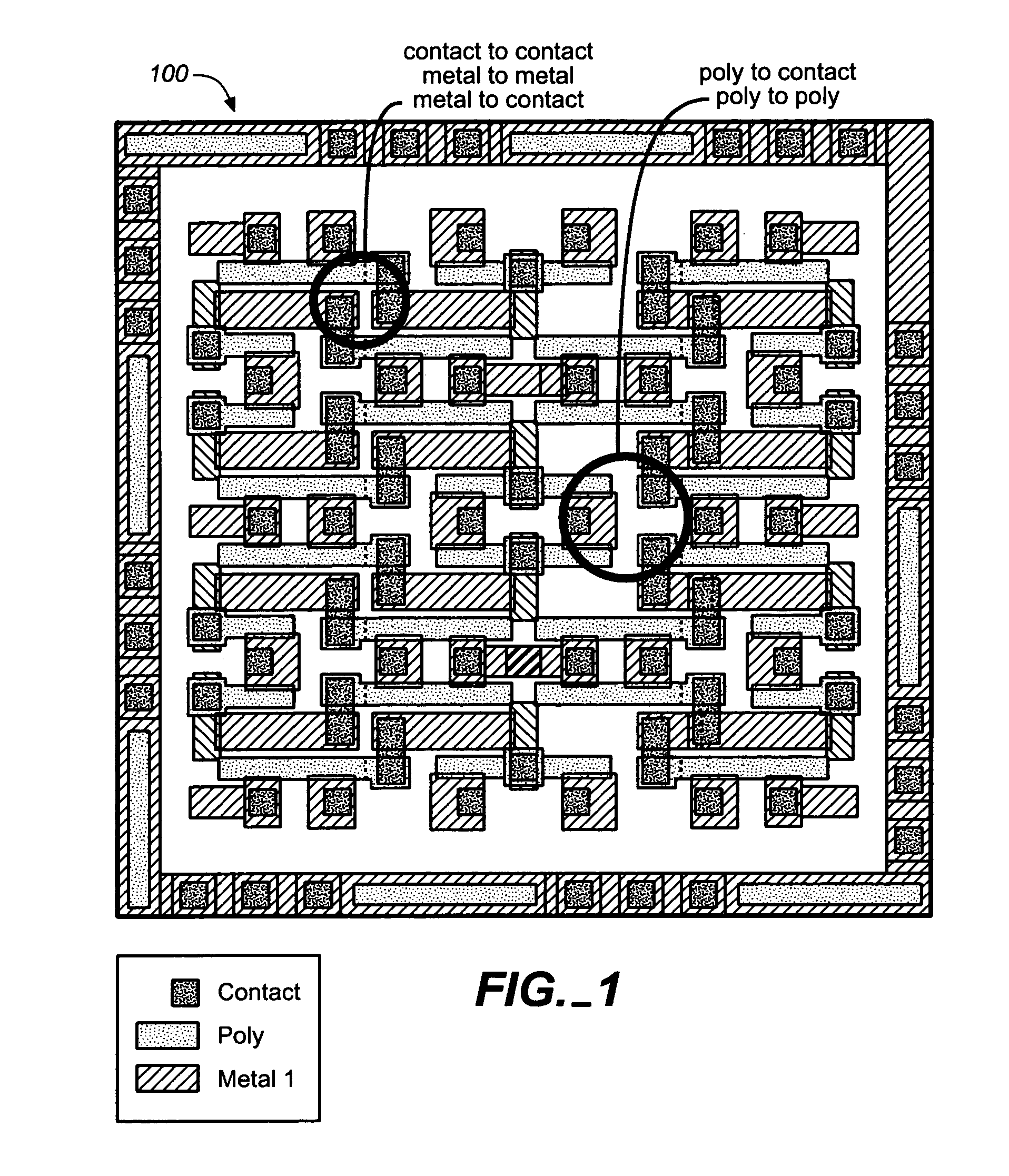
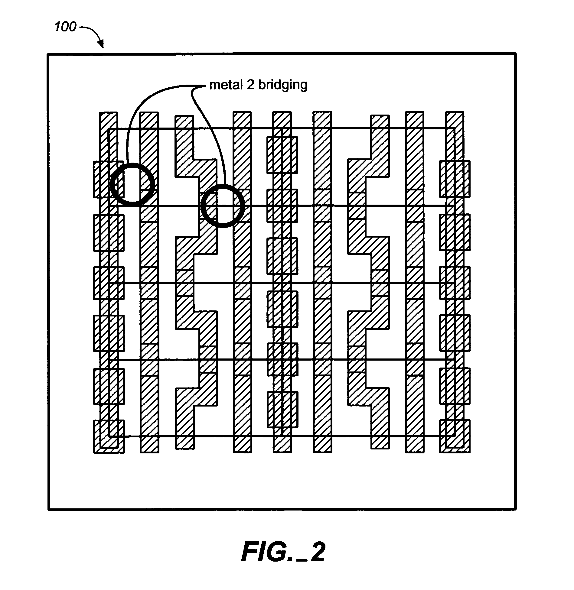
[0026]The present invention identifies two areas in a semiconductor integrated circuit to place more test structures for monitoring the semiconductor design and fabrication process. The first is a dummy area on a s...
PUM
 Abstract
Description
Claims
Application Information