Light emitting diode component

a technology of light emitting diodes and components, applied in the field of light arts, can solve the problems of low light output intensities low light output intensity of early light emitting diodes, and general inability to compete with incandescent and fluorescent light sources, and achieve relatively fragile light emitting packages

Inactive Publication Date: 2007-05-29
GENERAL ELECTRIC CO +1
View PDF79 Cites 261 Cited by
  • Summary
  • Abstract
  • Description
  • Claims
  • Application Information

AI Technical Summary

Benefits of technology

[0014]Numerous advantages and benefits of the present invention will become apparent to those of ordinary skill in the art upon reading and understanding the present specification.

Problems solved by technology

One issue with light emitting diode components or packages relates to light output intensity.
Early light emitting diodes had low light output intensities and were generally not competitive with incandescent and fluorescent light sources.
Another issue with light emitting diode components and packages relates to ruggedness.
Commonly used packaging techniques, such as bonding of the dice to lead frames, can produce relatively fragile light emitting packages.
Moreover, light emitting diode components and packages tend to be complex.
Multiple chip packages generally further increase complexity.
Baretz discloses a phosphor contained in an encapsulant disposed inside the housing, The complexity of multiple chip packages such as those of Lowery and Baretz can adversely impact manufacturability, reliability, and manufacturing costs.
Yet another issue with typical light emitting diode packages and components is operating lifetime.
Performance of packages employing phosphor wavelength conversion of ultraviolet or short-wavelength visible light typically degrades over time due to discoloration or other degradation of the encapsulant or other materials caused by the ultraviolet or short-wavelength visible light irradiation.

Method used


Image

  • Light emitting diode component
  • Light emitting diode component
  • Light emitting diode component

Examples


Embodiment Construction

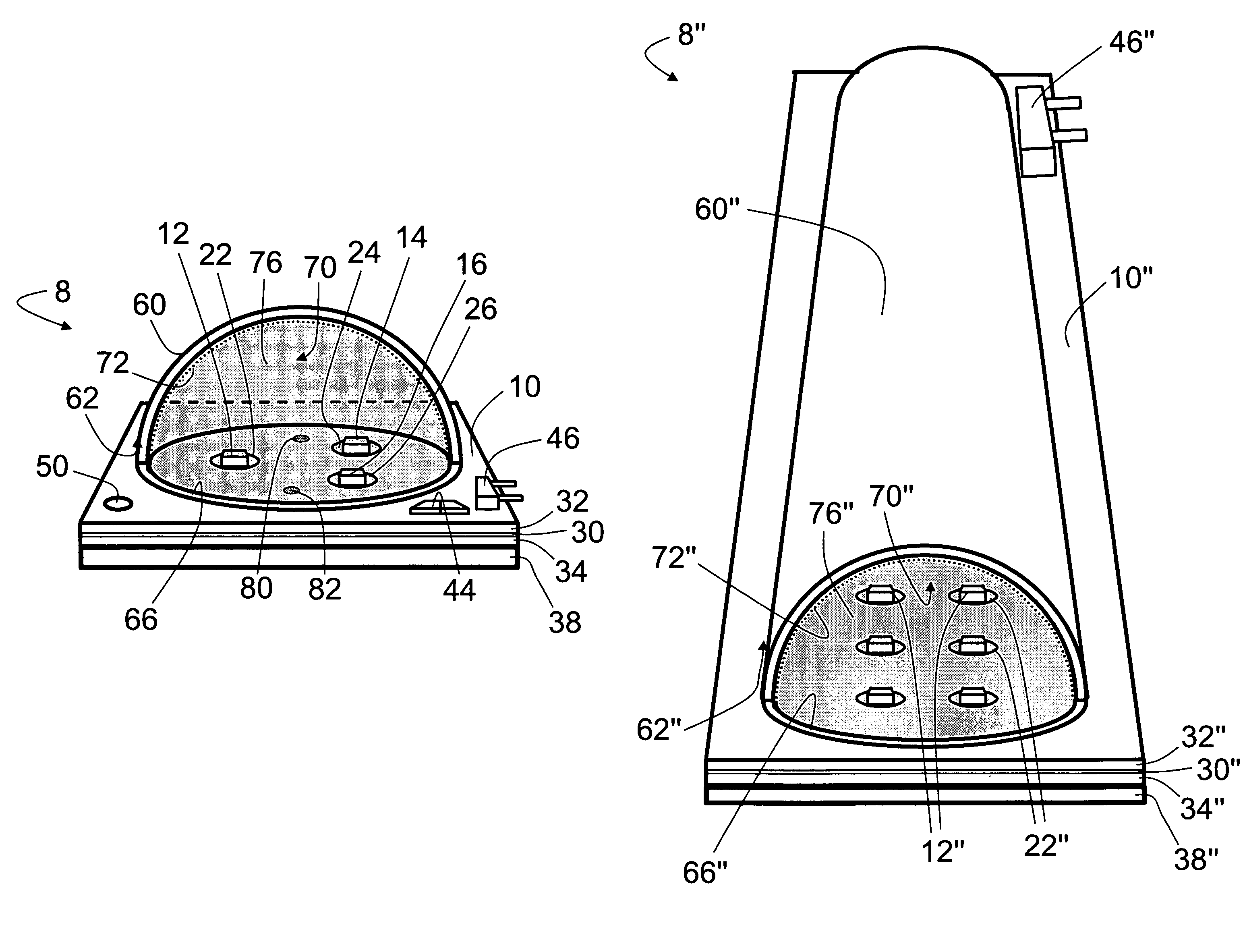
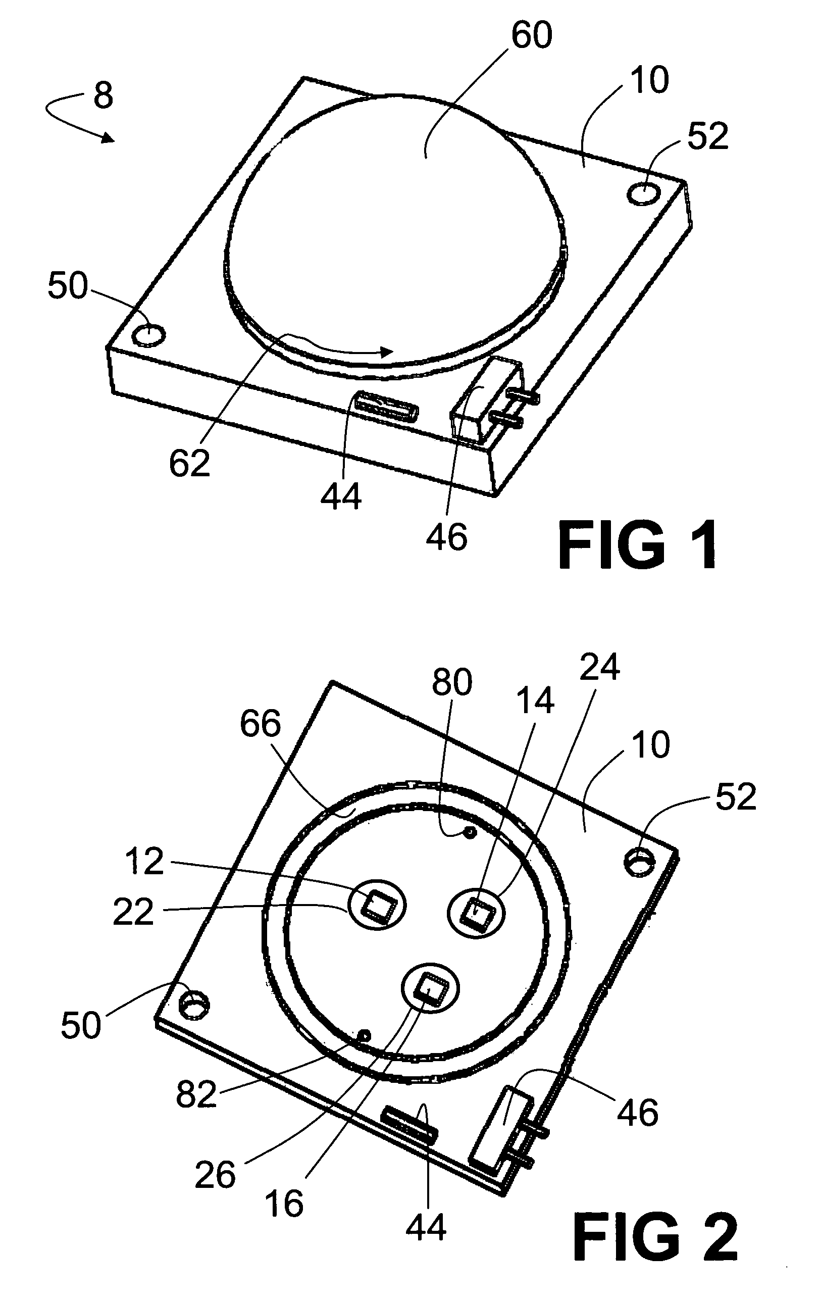
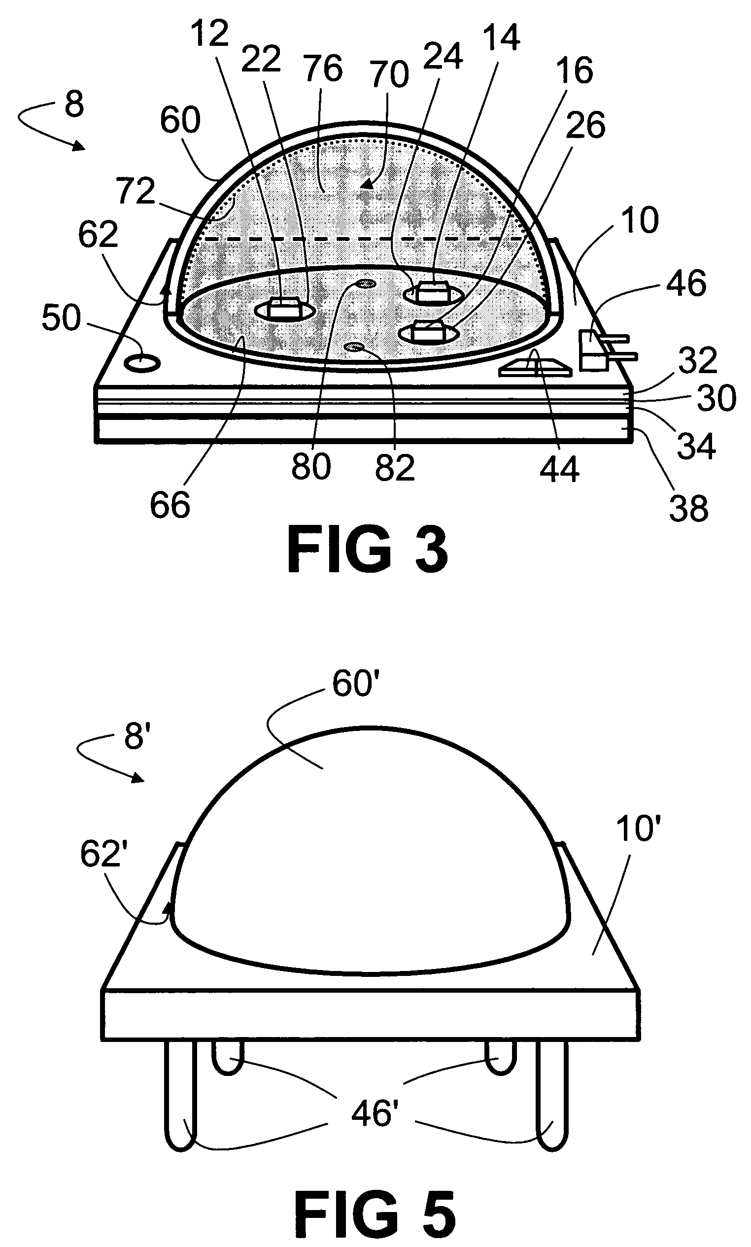
[0025]With reference to FIGS. 1–3, a light emitting package 8 includes a printed circuit board 10 on which one or more light emitting chips or die are disposed. The printed circuit board is preferably substantially thermally conductive. For example, a metal core printed circuit board can be employed. In the illustrated embodiment, three light emitting chips or dice 12, 14, 16 are disposed on the circuit board 10; however, the number of dice can be one die, two dice, or more than three dice. The die or dice can be group III-nitride blue or ultraviolet light emitting diodes, red group III-phosphide or group III-arsenide light emitting diodes, II–VI light emitting diodes, IV–VI light emitting diodes, silicon or silicon-germanium light emitting diodes, or the like. In some contemplated embodiments, the die or dice are edge emitting lasers or vertical cavity surface emitting lasers. The light emitting chips or dice can also be organic light emitting diodes or devices. Each light emitting...


PUM


Abstract

A light emitting package (8, 8′, 8″, 208, 408) includes a printed circuit board (10, 10′, 10″, 210, 410) supporting at least one light emitting die (12, 12″, 14, 16, 212, 412). A light transmissive cover (60, 60′, 60″, 260, 460) is disposed over the at least one light emitting die. The cover has an open end defining a cover perimeter (62, 62′, 62″, 262, 462) connected with the printed circuit board. An inside surface of the cover together with the printed circuit board defines an interior volume (70, 70″, 270, 470) containing the at least one light emitting die. An encapsulant (76, 76″, 276, 278, 476) is disposed in the interior volume and covers at least the light emitting die.

Description

[0001]This application is a continuation-in-part of International Application number PCT / US2003 / 027363 with an international filing date of Aug. 29, 2003 first published Mar. 11, 2004 as International Publication no. WO 2004 / 021461 A2, which claims the benefit of U.S. Provisional Application Ser. No. 60 / 407,426 filed on Aug. 30, 2002. This application incorporates by reference the content of International Application number PCT / US2003 / 027363. This application also incorporates by reference the content of U.S. Provisional Application Ser. No. 60 / 407,426.BACKGROUND[0002]The present invention relates to the lighting arts. It especially relates to single-chip and multiple-chip light emitting diode components and methods for making same, and will be described with particular reference thereto. However, the invention applies to light emitting packages generally, and is applicable in packaging monolithic light emitting diode array dice, edge-emitting laser dice, vertical cavity light emitt...

Claims


Application Information

Patent Timeline
Patent Type & Authority Patents(United States)
IPC IPC(8): H01L29/22H01L27/15H01L29/227H01L29/24H01L29/267H01L21/00H01L21/44H01L21/48H01L21/50H01L25/075H01L31/12H01L33/48H01L33/52H01L33/58
CPCH01L33/52H01L33/507H01L25/0753H01L33/483H01L2224/48091H01L33/58H01L2924/00
Inventor AANEGOLA, SRINATH K.PETROSKI, JAMES T.RADKOV, EMILWEAVER, JR., STANTON E.
Owner GENERAL ELECTRIC CO
Why Eureka
Try Eureka