Semiconductor inspection apparatus and manufacturing method of semiconductor device

a semiconductor device and semiconductor technology, applied in the direction of electrical testing, measurement devices, instruments, etc., can solve the problems of short circuit in the wiring, generation of foreign substances, rough electrodes, etc., to ensure the positional accuracy of the tips, improve the electrical properties and reliability, and ensure the contact resistance value stable

Inactive Publication Date: 2007-06-05
RENESAS ELECTRONICS CORP
View PDF5 Cites 26 Cited by
  • Summary
  • Abstract
  • Description
  • Claims
  • Application Information

AI Technical Summary

Benefits of technology

[0015]An object of the present invention is to provide technologies which can ensure the positional accuracy of the tips of contact terminals and can inspect a plurality semiconductor elements formed on a wafer at one time with stable contact resistance values.
[0016]Another object of the present invention is to provide a structure in which electronic components for inspection circuits can be mounted in the vicinity of contact terminals and to provide technologies which can improve the electrical properties and reliability.
[0017]Still another object of the present invention is to provide technologies which can reduce the overall manufacturing cost of semiconductor devices by improving assembly performance of a probe sheet on which contact terminals are formed, simplifying procedures and operations of inspection process, and reducing the assembly cost of the inspection apparatus to reduce the cost of inspection process of semiconductor devices.
[0020]In an aspect of the present invention, by reducing the pressure of the space formed between the probe sheet and the target to be inspected facing to each other, the target to be inspected is mainly deformed to bring the contact terminals of the probe sheet into contact with electrodes of the target to be inspected. In this state, plural circuit units of the target to be inspected are electrically inspected.
[0021]Also, the present invention provides a semiconductor inspection apparatus comprising: (a) a support member supporting a semiconductor wafer having a first principal surface and a second principal surface which is on the other side of the first principal surface, a plurality of semiconductor chips formed on the first principal surface, and a plurality of electrodes disposed on each of the plurality of semiconductor chips; (b) a probe sheet having a third principal surface facing the first principal surface of the semiconductor wafer with a desired space provided therebetween, a fourth principal surface which is on the other side of the third principal surface, a plurality of contact terminals disposed on the third principal surface, a plurality of wirings respectively led from the plurality of contact terminals, and a plurality of lead electrodes led to the fourth principal surface via the plurality of wirings; (c) a tester connected to the plurality of lead electrodes of the probe sheet and electrically inspecting the plurality of semiconductor chips of the semiconductor wafer at one time; and (d) pressure reducing means for reducing the pressure of the desired space in the inspection so that the semiconductor wafer is mainly deformed to bring the plurality of electrodes of the plurality of semiconductor chips of the semiconductor wafer into contact with the plurality of contact terminals of the probe sheet.

Problems solved by technology

As a result, scratching the electrode with the contact terminals generates dusts of the electrode material, and causes short-circuit in the wirings and generation of foreign substances.
Moreover, since contact is achieved by scratching the electrodes with the probes while applying a load of several hundred mN or more to the electrodes, the electrodes are often damaged.
In addition, at the time of the wire bonding or formation of connection bumps to be performed on the electrodes after the probing, rough electrode surface causes connection failure.
As a result, the reliability is degraded.
Moreover, in the inspection process using such a probe card, since the disposal of probes has spatial limit, the probe card cannot deal with the density increase and narrower pitches of electrode pads for inspection of semiconductor devices, the increase in the number of electrode pads, and the positional accuracy of the probe tips in a large area.
Moreover, in the above-described probing method, bare probe length is long due to the shape and relative arrangement of the probes, cross talk occurs, and the waveforms are disturbed when high-speed signals are used.
Therefore, accurate inspection cannot be performed.
More specifically, it becomes impossible to deal with the inspection of semiconductor devices in which signal processing speed is increasing more and more in the future.
However, it is difficult to handle the case when a plurality of semiconductor elements in a wafer state are to be simultaneously inspected at one time, because electronic components (resistances, capacitors, fuses, and others) for inspection circuits have to be mounted as close as possible to each of the semiconductor elements.
In addition, this technology has a problem that fine adjustment of the applied load is difficult since contact pressure load is controlled only by applying the pressure to the buffer layer.

Method used


Image

  • Semiconductor inspection apparatus and manufacturing method of semiconductor device
  • Semiconductor inspection apparatus and manufacturing method of semiconductor device
  • Semiconductor inspection apparatus and manufacturing method of semiconductor device

Examples


Embodiment Construction

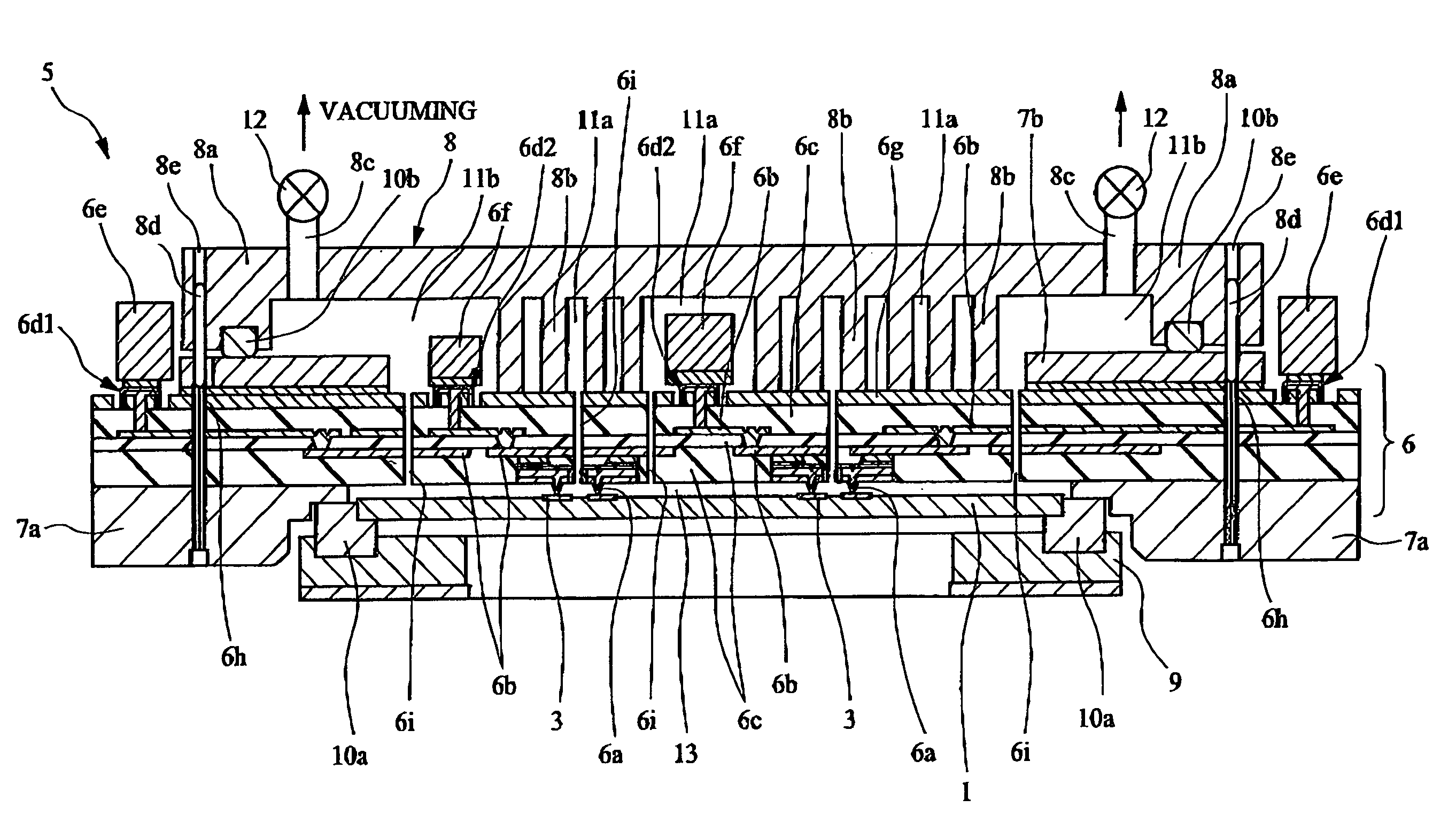
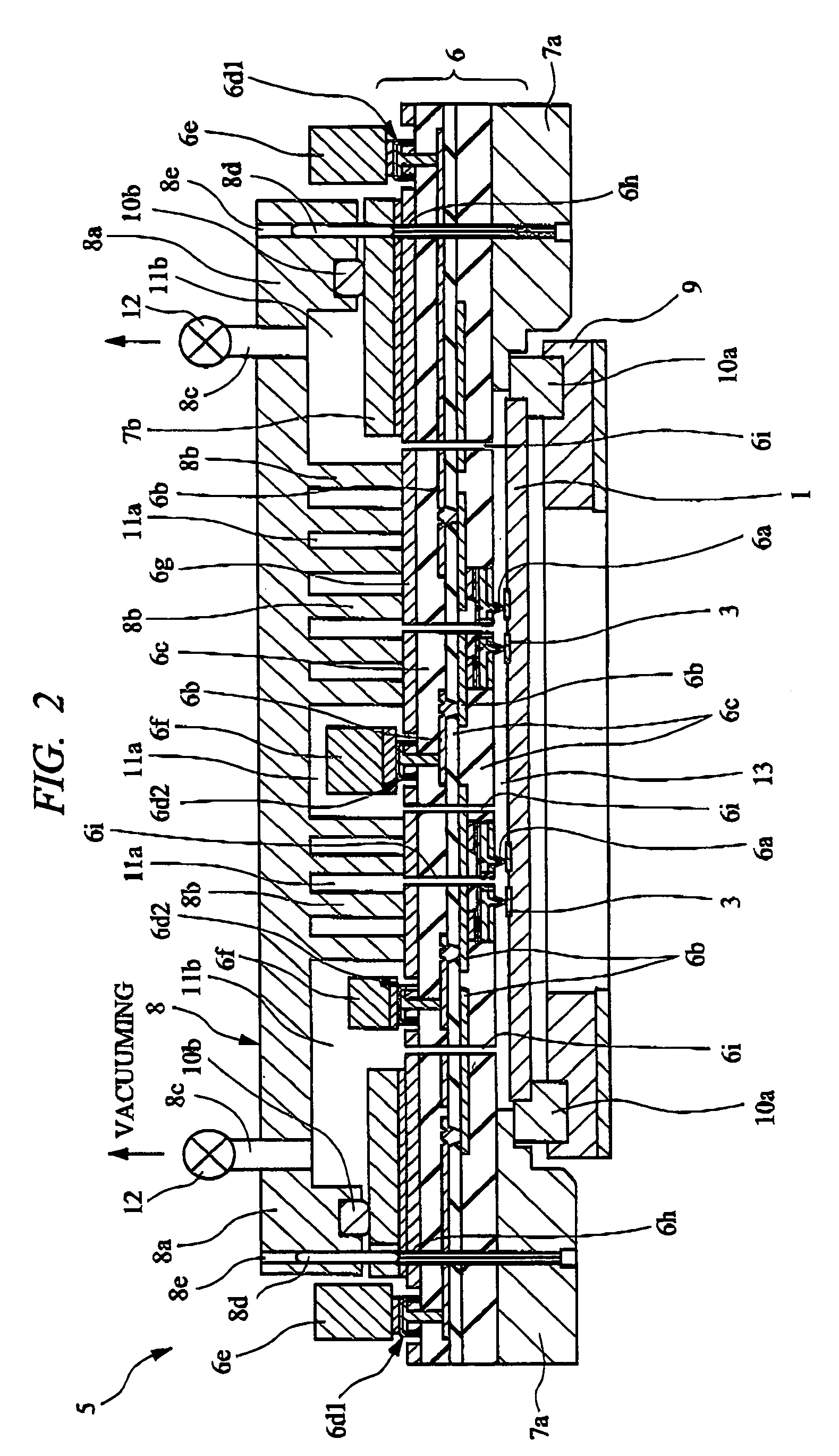
[0066]Hereinafter, embodiments of the present invention will be described in detail with reference to the accompanying drawings. In the embodiments described below, the invention will be described in a plurality of sections or embodiments when required as a matter of convenience. However, these sections or embodiments are not irrelevant to each other unless otherwise stated, and the one relates to the entire or a part of the other as a modification example, details, or a supplementary explanation thereof. Also, components having the same function are denoted by the same reference symbols throughout the drawings for describing the embodiments, and the repetitive description thereof is omitted.

[0067]Also, in the embodiments of the present invention, main terms are defined as follows.

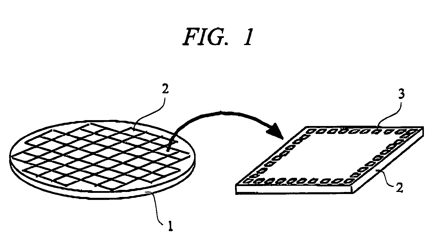
[0068]Regardless of the form thereof, semiconductor devices include the devices in a wafer state in which circuits are formed (for example, a semiconductor wafer (hereinafter, simply referred to as a wafer...


PUM


Abstract

When electrical properties of semiconductor chips of a semiconductor wafer are inspected by bringing plural contact terminals disposed on the principal surface of a probe sheet of a probe cassette constituting a semiconductor inspection apparatus into contact with plural electrodes of the plural semiconductor chips on the principal surface of the semiconductor wafer which is disposed so as to face the principal surface of the probe sheet, the air pressure of the space formed between the facing surfaces of the principal surface of the probe sheet and the principal surface of the semiconductor wafer is reduced so as to suck the semiconductor wafer toward the side of the principal surface of the probe sheet and deform mainly the semiconductor wafer, thereby pressing the plural electrodes of the plural semiconductor chips of the semiconductor wafer against the plural facing contact terminals of the principal surface of the probe sheet.

Description

CROSS-REFERENCE TO RELATED APPLICATION[0001]The present application claims priority from Japanese Patent Application No. JP 2004-378504 filed on Dec. 28, 2004, the content of which is hereby incorporated by reference into this application.TECHNICAL FIELD OF THE INVENTION[0002]The present invention relates to a semiconductor inspection apparatus and a manufacturing technology of a semiconductor device. More particularly, it relates to a technology effectively applied to a semiconductor inspection apparatus using a probe sheet and a manufacturing method of a semiconductor device using the semiconductor inspection apparatus.BACKGROUND OF THE INVENTION[0003]As the manufacturing technologies of semiconductor devices, the following technologies are known.[0004]For example, in the manufacturing process of a semiconductor device, after forming semiconductor circuits on a wafer, an assembly step is carried out, through which products such as packaged products, bare chips, and CSPs (Chip Size...

Claims


Application Information

Patent Timeline
Patent Type & Authority Patents(United States)
IPC IPC(8): G01R31/02
CPCG01R31/2886G01R1/0491
Inventor KASUKABE, SUSUMU
Owner RENESAS ELECTRONICS CORP
Why Eureka
Try Eureka