Method for doping structures in FinFET devices

a technology of finfet and structure, applied in the field of forming finfet devices, can solve the problems of increasing difficulty in overcoming, short channel effect, excessive leakage between source and drain, etc., and achieve the effect of low source-drain resistan

Inactive Publication Date: 2007-06-26
GLOBALFOUNDRIES INC
View PDF4 Cites 39 Cited by
  • Summary
  • Abstract
  • Description
  • Claims
  • Application Information

AI Technical Summary

Benefits of technology

[0005]Implementations consistent with the principles of the invention use doped glass to uniformly dope the fin

Problems solved by technology

The reduction of design features below 100 nm challenges the limitations of conventional methodology.
For example, when the gate length of conventional planar metal oxide semiconductor field effect transistors (MOSFETs) is scaled below 100 nm, problems associated with short cha

Method used


Image

  • Method for doping structures in FinFET devices
  • Method for doping structures in FinFET devices
  • Method for doping structures in FinFET devices

Examples


Embodiment Construction

[0013]The following detailed description of implementations consistent with the present invention refers to the accompanying drawings. The same reference numbers in different drawings may identify the same or similar elements. Also, the following detailed description does not limit the invention. Instead, the scope of the invention is defined by the appended claims and their equivalents.

[0014]Implementations consistent with the principles of the invention use doped glass to uniformly dope the fin structure and source / drain regions of FinFET devices. As a result, low source-drain resistance can be achieved.

Exemplary Processing

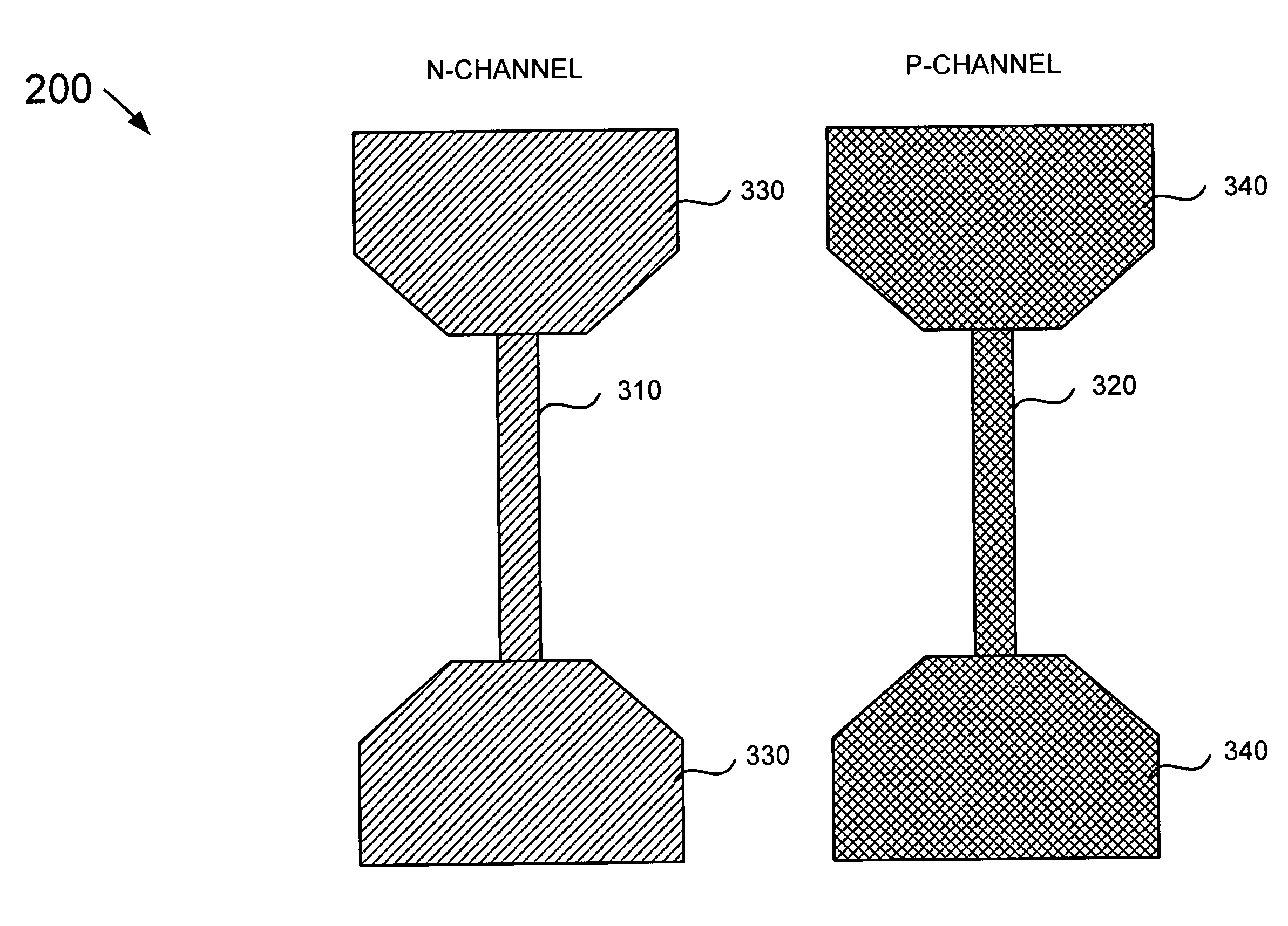
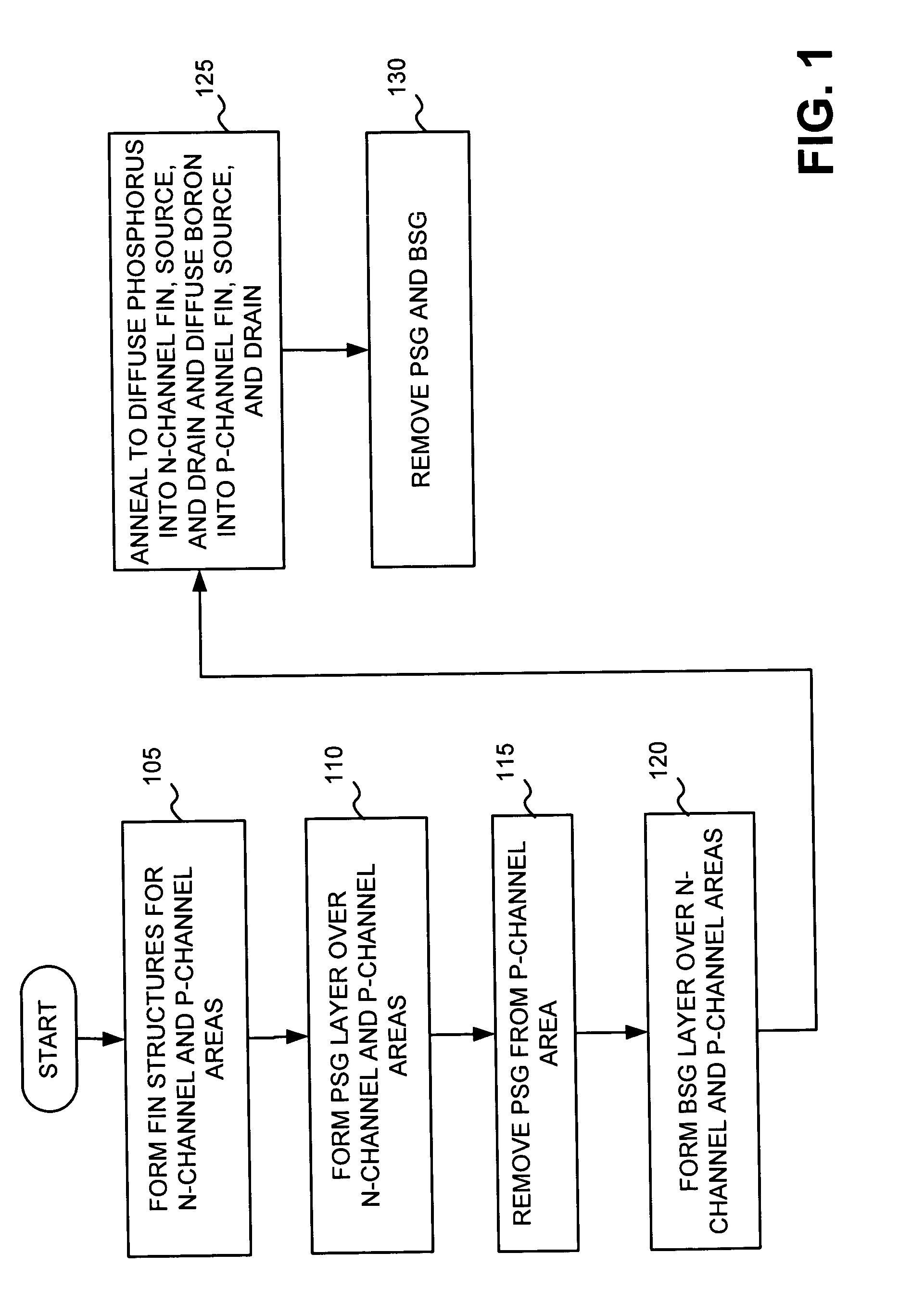
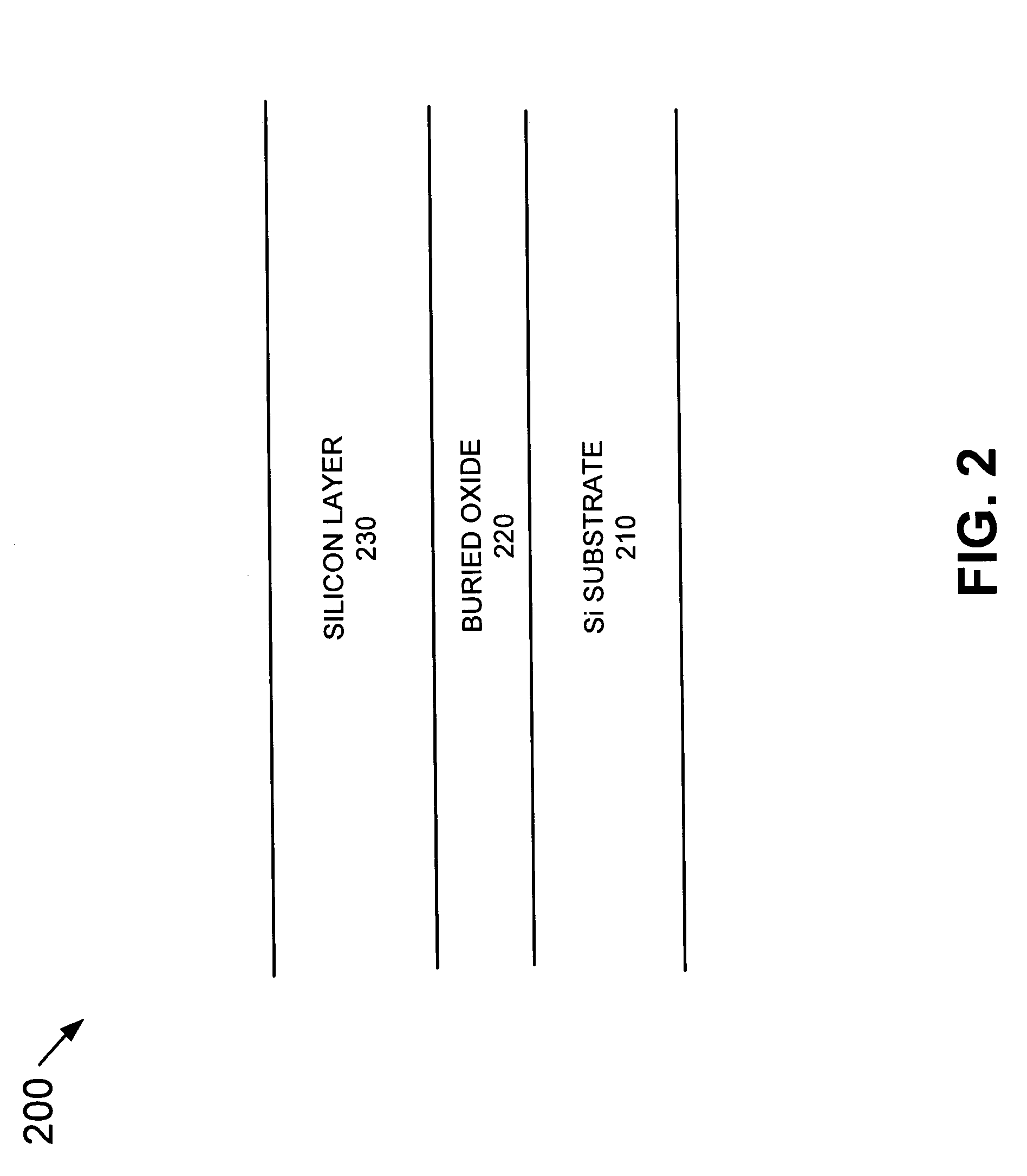
[0015]FIG. 1 illustrates an exemplary process for forming FinFET devices in an implementation consistent with the principles of the invention. FIGS. 2–7B illustrate exemplary views of FinFET devices fabricated according to the processing described in FIG. 1. The fabrication of two FinFET devices will be described hereinafter. It will be appreciated, however, tha...


PUM


Abstract

A method for doping fin structures in FinFET devices includes forming a first glass layer on the fin structure of a first area and a second area. The method further includes removing the first glass layer from the second area, forming a second glass layer on the fin structure of the first area and the second area, and annealing the first area and the second area to dope the fin structures.

Description

FIELD OF THE INVENTION[0001]The present invention relates generally to semiconductor manufacturing and, more particularly, to forming FinFET devices.BACKGROUND OF THE INVENTION[0002]The escalating demands for high density and performance associated with ultra large scale integration semiconductor devices require design features, such as gate lengths, below 100 nanometers (nm), high reliability and increased manufacturing throughput. The reduction of design features below 100 nm challenges the limitations of conventional methodology.[0003]For example, when the gate length of conventional planar metal oxide semiconductor field effect transistors (MOSFETs) is scaled below 100 nm, problems associated with short channel effects, such as excessive leakage between the source and drain, become increasingly difficult to overcome. In addition, mobility degradation and a number of process issues also make it difficult to scale conventional MOSFETs to include increasingly smaller device feature...

Claims


Application Information

Patent Timeline
IPC IPC(8): H01L21/84
CPCH01L21/845H01L27/1211H01L29/66795H01L29/785H01L29/66803
Inventor LIN, MING-RENKRIVOKAPIC, ZORANWANG, HAIHONGYU, BIN
Owner GLOBALFOUNDRIES INC
Why Eureka
Try Eureka