

Probe station comprising a bellows with EMI shielding capabilities
a technology of emi shielding and bellows, which is applied in the field of probe stations, can solve the problems of slot antennas which jeopardize effective emi shielding, can not be easily assembled, and the assembly is complicated and expensive, so as to improve the performance and reduce the manufacturing cost , the effect of easy compensation of the movement of the prob
- Summary
- Abstract
- Description
- Claims
- Application Information
AI Technical Summary
Benefits of technology
Problems solved by technology
Method used
Image

Examples
Embodiment Construction
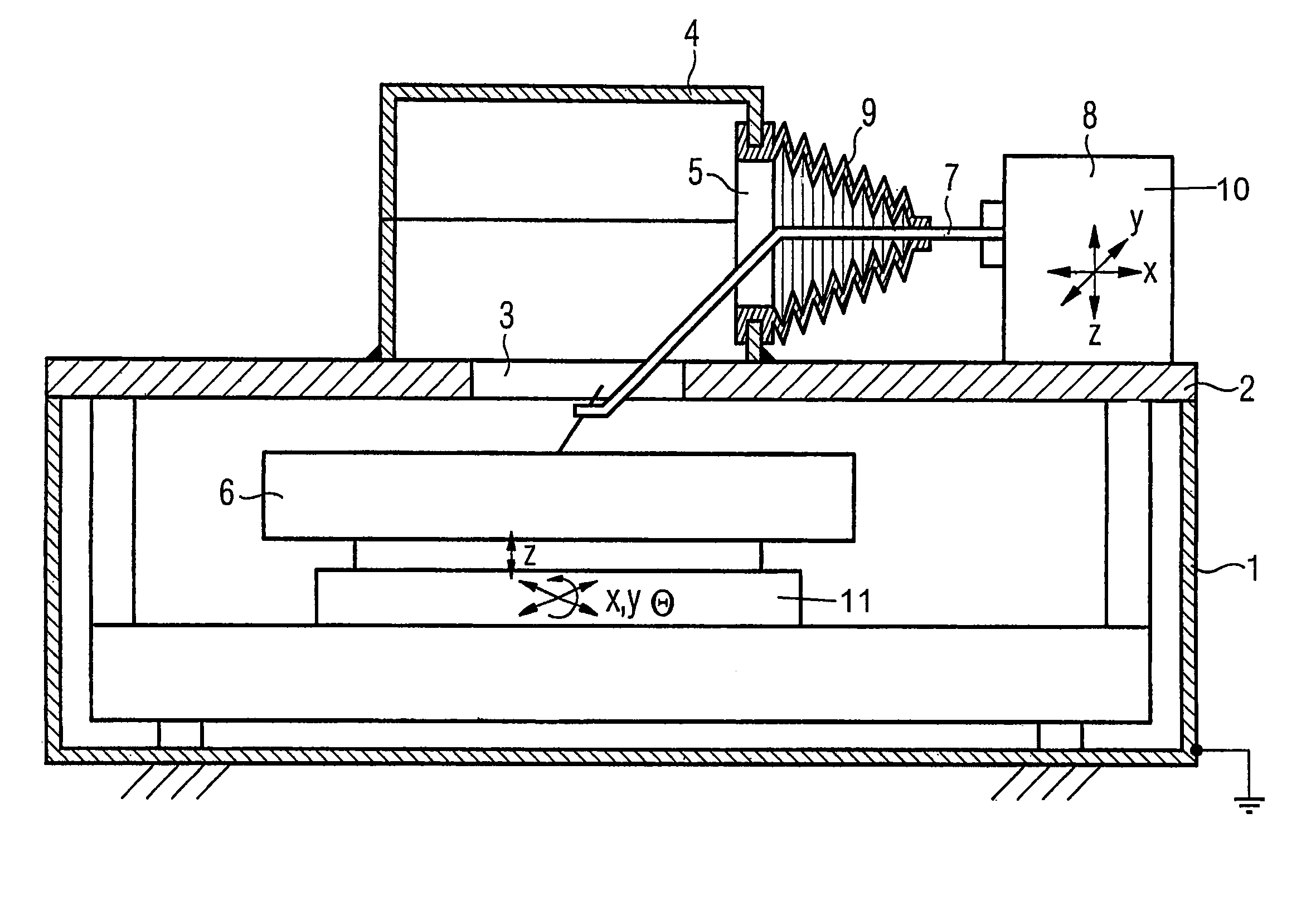
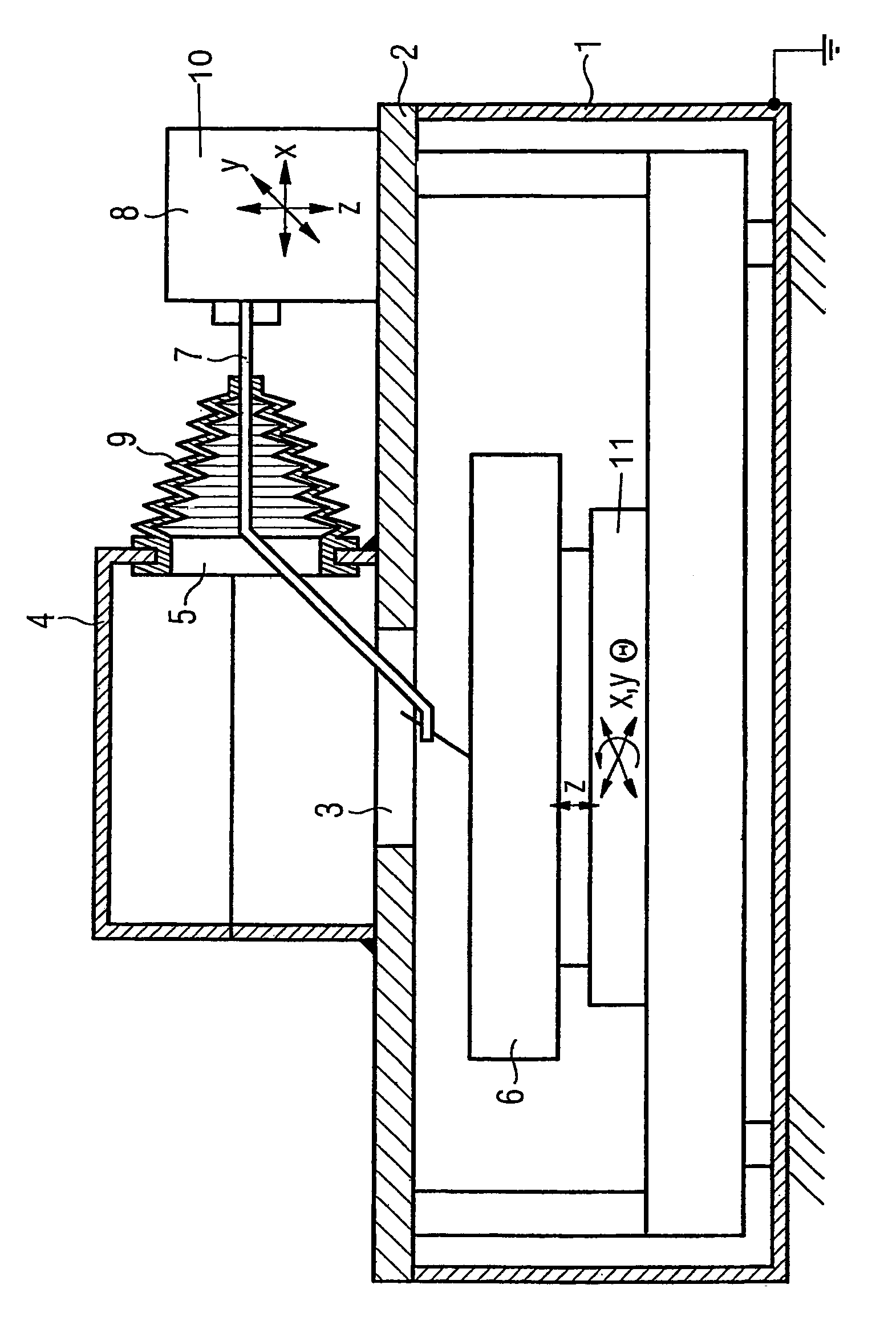
[0023]With reference to the FIGURE, an exemplary embodiment of the probe station of the present invention comprises a housing 1 having an aperture 5 through which a probe 7 extends. The aperture 5 is arranged in a covering structure 4 covering an opening 3 in a top wall 2 of the housing 1. The probe 7 is supported by a probe support 8 which is arranged in close proximity to the covering structure 4 so that the first portion of the probe 7 extends into the housing 1 through the aperture 5. Inside the housing 1 there is arranged a chuck 6 for supporting a test device (not shown). Two independent positioning mechanisms 10 and 11 enable both the probe 7 and the chuck 6 to move relative to the other.
[0024]An electrically conductive elastic bellows 9 extends between the position where it is fixed to the outside portion of the probe 7 and the aperture 5 of the housing 1 such that the elastic bellows 9 is in close contact with the probe 7. The elastic bellows 9 is of substantially conical s...
PUM
 Abstract
Description
Claims
Application Information