Method for manufacturing chip resistor

a technology of resistor and chip, which is applied in the direction of resistors adapted for terminal application, resistive material coating, manufacturing tools, etc., can solve the problems of dimensional errors and difficult manufacturing of resistors

Inactive Publication Date: 2007-07-03
PANASONIC CORP
View PDF18 Cites 13 Cited by
  • Summary
  • Abstract
  • Description
  • Claims
  • Application Information

AI Technical Summary

Problems solved by technology

This method may cause a variation in the composition of the substrate 120 and a change in its baking temperature, thus resulting in dimensional errors of the longitudinal slit lines 122, the traverse slit lines 123, and the oval apertures 128.
The screen printing masks have to be replaced from one to another with reference to the levels of the dimensional classification of the chips on the substrate, thus making the resistor hard to manufacture.

Method used


Image

  • Method for manufacturing chip resistor
  • Method for manufacturing chip resistor
  • Method for manufacturing chip resistor

Examples


exemplary embodiment 1

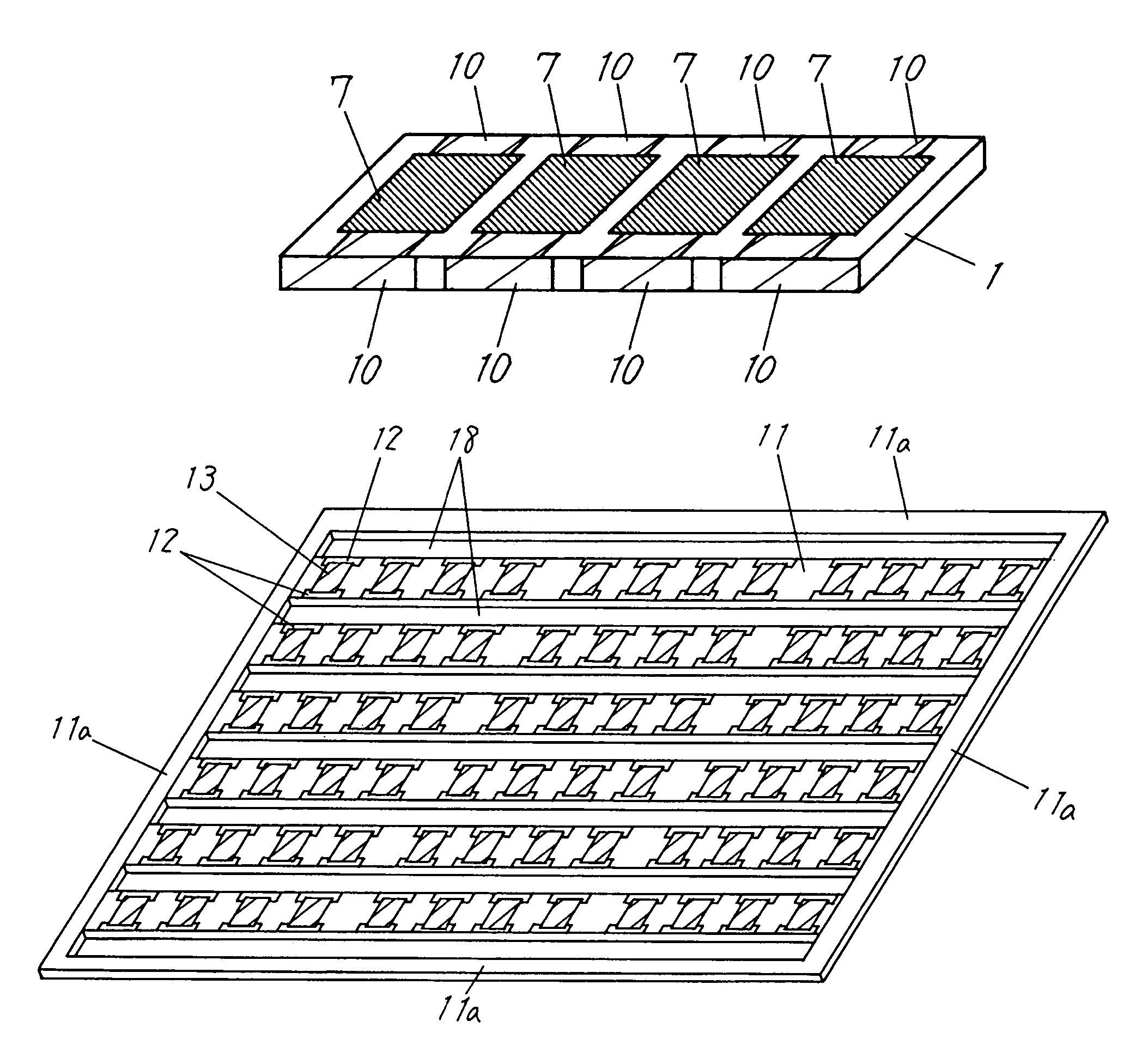
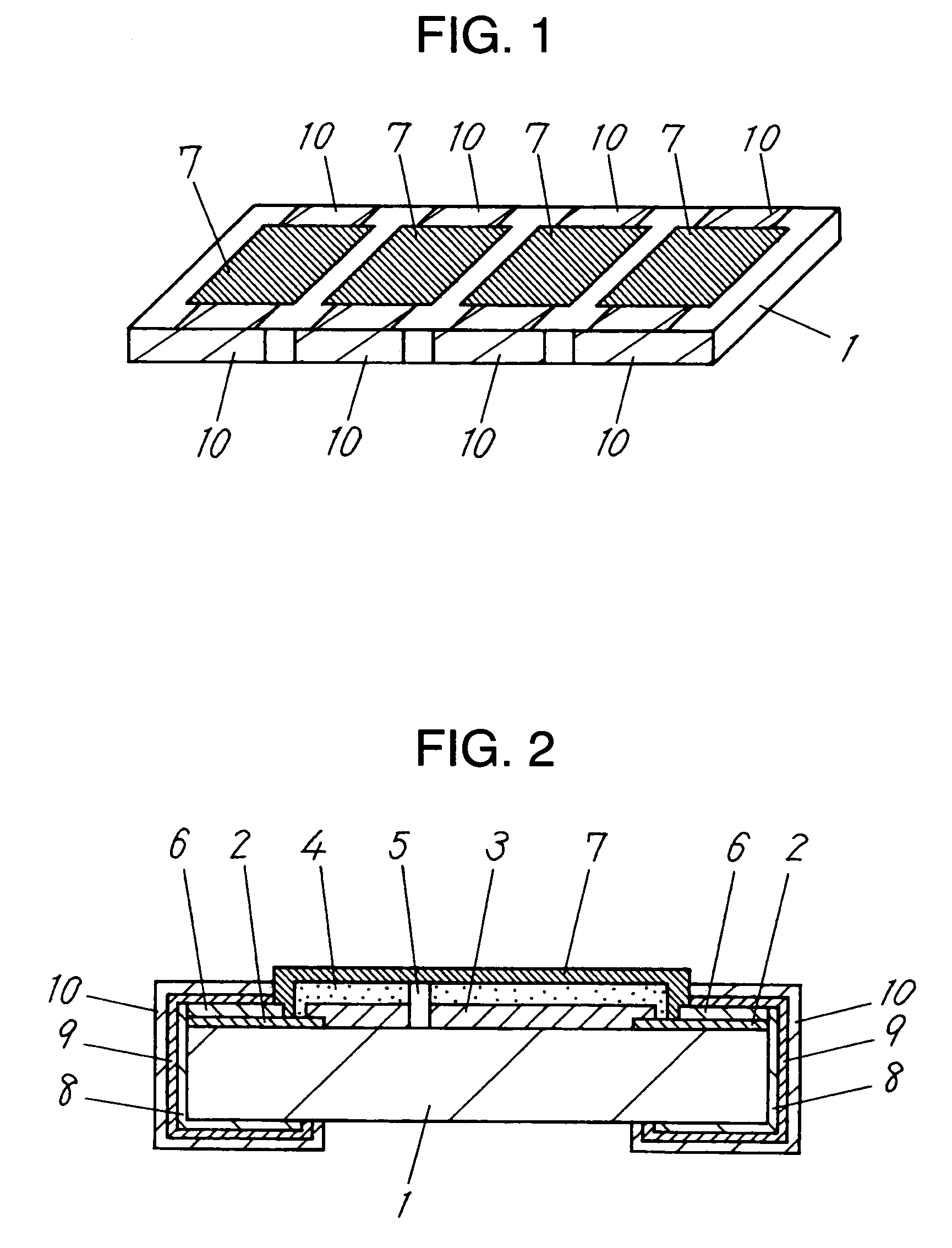
[0039]FIG. 1 is a perspective view of a multiple chip resistor manufactured by a method according to Exemplary Embodiment 1 of the present invention. FIG. 2 is a cross sectional view of the resistor. The resistor includes a substrate 1 separated from a substrate shaped in a sheet of baked aluminum of 96% purity by dividing the substrate along first dividing sections and second dividing sections orthogonal to the first dividing sections. The substrate 1 has pairs of upper electrode layers 2 made of silver-based material provided on the upper surface of the substrate 1. The substrate 1 includes resistor elements 3 made of ruthenium oxide material provided on the upper surface of the substrate 1. The resistor elements 3 partially overlap, i.e., are electrically connected to the upper electrode layers 2. The resistor elements 3 are covered entirely with first protective layers 4 made of glass-based material, respectively. The resistor element 3 and the first protective layer 4 have a tr...

embodiment 2

[0074]A method of manufacturing a multiple chip resistor according to Exemplary Embodiment 2 of the present invention will be described by referring to relevant figures. The method of Embodiment 2 is differentiated from that of Embodiment 1 by some processes which are explained in detail while the description of other identical processes is omitted. More particularly, the method of Embodiment 2 is identical to that of Embodiment 1 before a process of providing back electrodes 20 shown in FIGS. 14 and 15. Processes after the process will be described while like components are denoted by like numerals as those of Embodiment 1.

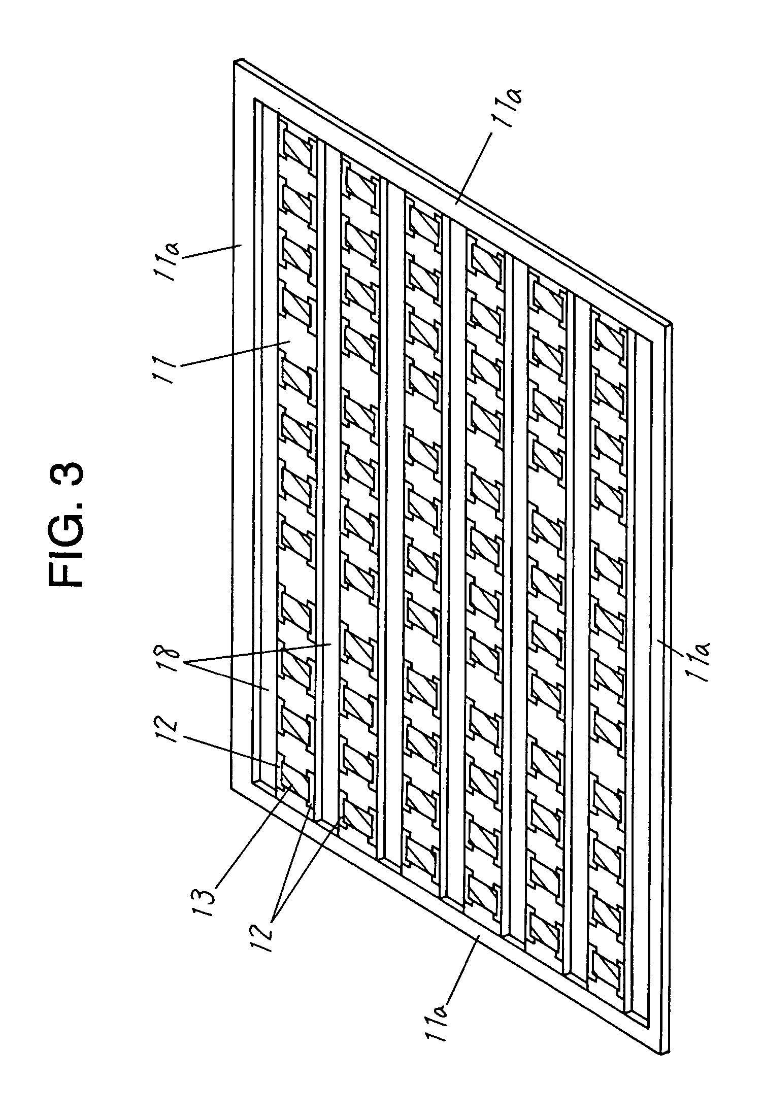
[0075]After being provided with the back electrodes 20 shown in FIGS. 14 and 15, the sheet substrate 11 having second protective layers 17, edge electrodes 19, and the back electrodes 20 are tiled so that the second protective layers 17 face down, as shown in FIG. 24. The edge electrodes and the back electrodes 20 include unnecessary portions between resistor ele...


PUM

PropertyMeasurementUnit
thicknessaaaaaaaaaa
peak temperatureaaaaaaaaaa
temperatureaaaaaaaaaa

Abstract

A multiple chip resistor is manufactured in the following method. First electrode layers are formed on a first surface of a substrate. Resistor elements electrically connected to the first electrode layers, respectively, are formed on the first surface of the substrate. Slits are formed in the substrate for separating the first electrode layers. Edge electrodes connected to the first electrode layers at the edges of the slits, respectively, are formed on respective edges at the slits of the substrate. The substrate is divided at the slits into strip substrates. Portions of the edge electrodes are removed for electrically isolating the resistor elements from each other. The method provides the edge electrodes on each strip substrate with an improved dimensional accuracy, hence allowing the edge electrodes to be isolated electrically from each other. Consequently, the multiple chip resistor is prevented from being mounted defectively when the resistor is surface-mounted.

Description

[0001]THIS APPLICATION IS A U.S. NATIONAL PHASE APPLICATION OF PCT INTERNATIONAL APPLICATION PCT / JP03 / 00195.FIELD OF THE INVENTION[0002]The present invention relates to a method of manufacturing a multiple chip resistor having an array of resistor elements provided on a single substrate.BACKGROUND OF THE INVENTION[0003]A conventional method of manufacturing a multiple chip resistor is disclosed in Japanese Utility Model Laid-Open No. 3-30409 as shown in FIGS. 31 to 33. In the method, both sides of a substrate 120 of a pre-baked green sheet of, e.g., a ceramic material is provided with longitudinal slit lines 122 and traverse slit lines 123. The substrate is separated along the longitudinal slit lines 122 into rectangular strips each of which includes chips 121 which are connected. Each strip is separated along the traverse slit lines 123 into the chips 121. Substantially-oval apertures 128 are provided at the intersections between the longitudinal slit lines 122 and the traverse sli...

Claims


Application Information

Patent Timeline
Patent Type & Authority Patents(United States)
IPC IPC(8): H01C17/06H01C1/142H01C7/00H01C17/00
CPCH01C1/142H01C7/003H01C17/006Y10T29/49789Y10T29/49099Y10T29/49082Y10T29/49101H01C17/06
Inventor MATSUKAWA, TOSHIKIKINOSHITA, YASUHARUHOSHITOKU, SHOJITAKAHASHI, MASAHARUANDO, YOSHINORI
Owner PANASONIC CORP
Why Eureka
Try Eureka