

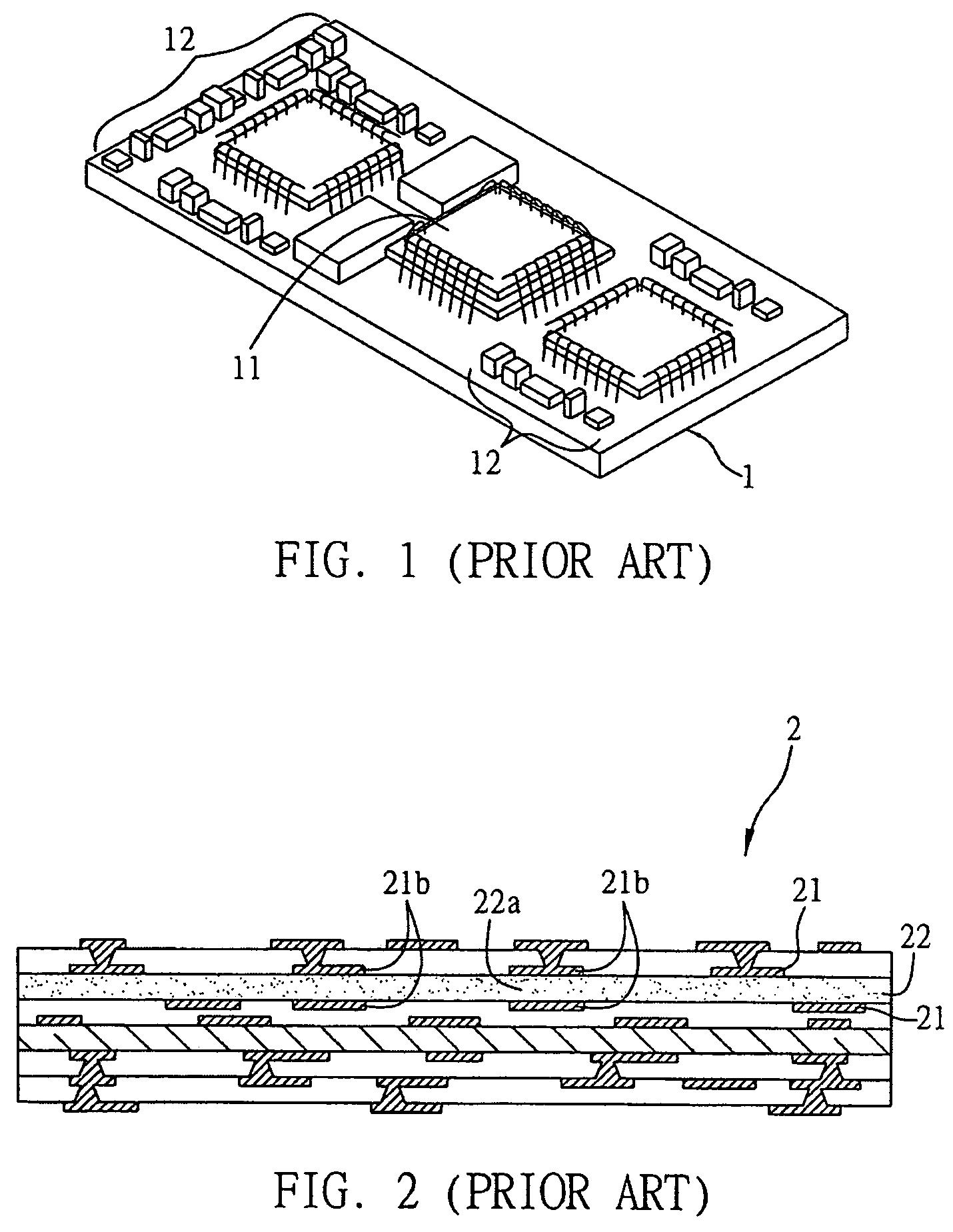
Circuit board structure with embedded selectable passive components and method for fabricating the same
a selectable passive component and circuit board technology, applied in the association of printed circuit non-printed electric components, conductive pattern formation, electrical apparatus construction details, etc., can solve the problems of increasing the overall size of the product incorporating the circuit board, increasing the complexity of the circuit layout and fabrication process of the semiconductor device, and increasing the generation of nois
- Summary
- Abstract
- Description
- Claims
- Application Information
AI Technical Summary
Benefits of technology
Problems solved by technology
Method used
Image

Examples
Embodiment Construction
[0022]The following special embodiment is provided to illustrate the present invention. Other advantages and effects can be understood by those in the art after reading the disclosure of this specification. The present invention can also be performed or applied by other embodiments. The details of the specification are provided using a particular application, and numerous modifications and variations can be devised without departing from the spirit of the present invention. It should be noted that the drawings of the present invention are simplified for the sake of easy illustration and are not drawn according to actual dimensions, and, therefore, do not show the real sizes or relative distances of the associated components.
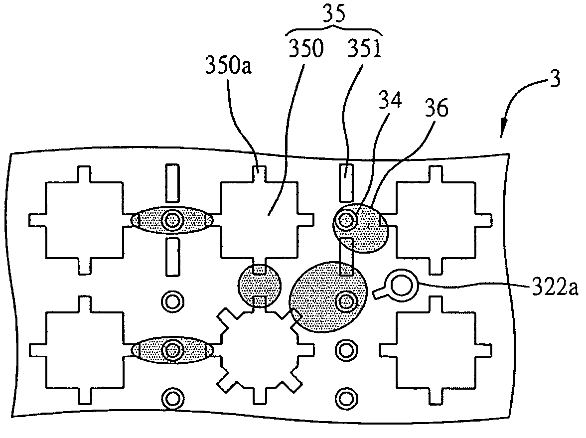
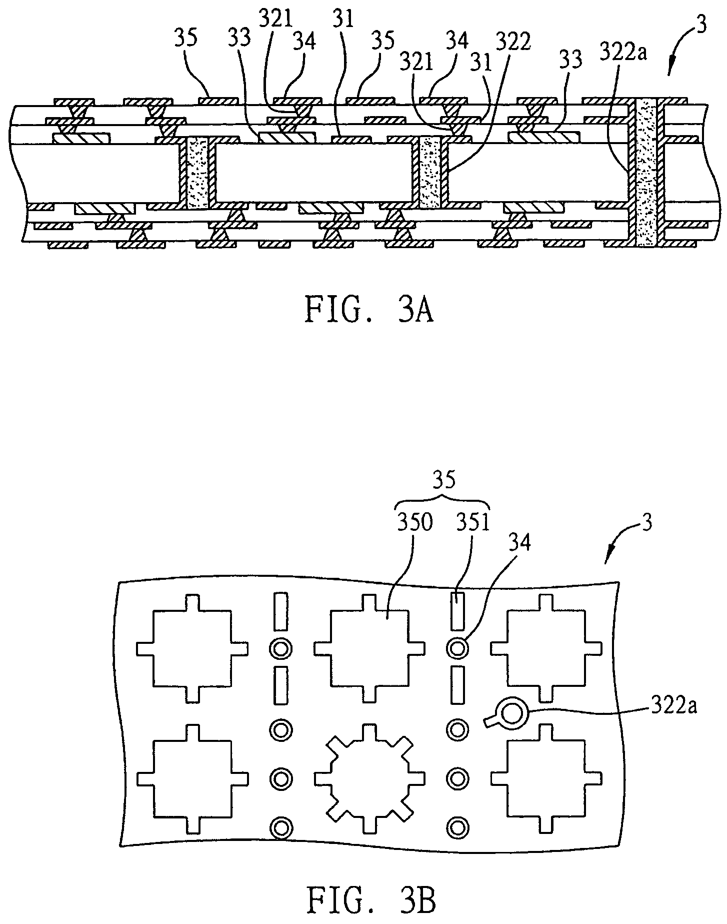
[0023]FIGS. 3A, 3B and FIG. 4 are schematic diagrams showing the method for fabricating the circuit board structure with embedded selectable passive components.
[0024]As shown in FIG. 3A, a multi-layer circuit board 3 is provided. The circuit board 3 includes a pl...
PUM
| Property | Measurement | Unit |
|---|---|---|
| dielectric constant | aaaaa | aaaaa |
| electric | aaaaa | aaaaa |
| conductive | aaaaa | aaaaa |
Abstract
Description
Claims
Application Information