Method for fabricating a structure for a microelectromechanical system (MEMS) device

a technology of microelectromechanical systems and structures, applied in the field of microfabrication, can solve the problems of adding to the cost of the device, each masking step,

Inactive Publication Date: 2007-07-31
SNAPTRACK
View PDF467 Cites 81 Cited by
  • Summary
  • Abstract
  • Description
  • Claims
  • Application Information

AI Technical Summary

Problems solved by technology

When manufacturing a MEMS device usually several masking steps are required, each masking step adding to the cost of the device.

Method used


Image

  • Method for fabricating a structure for a microelectromechanical system (MEMS) device
  • Method for fabricating a structure for a microelectromechanical system (MEMS) device
  • Method for fabricating a structure for a microelectromechanical system (MEMS) device

Examples


Embodiment Construction

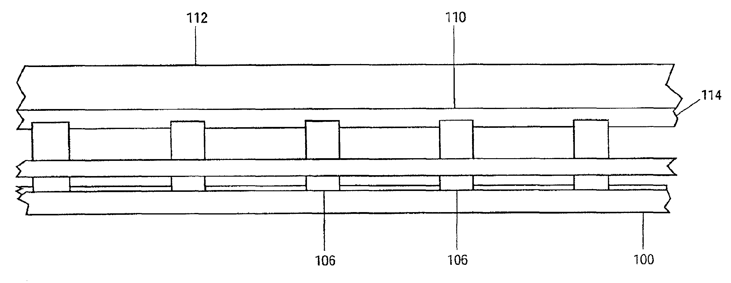
[0007]Aspects of the present invention will now be described with reference to FIGS. 2 to 10 of the drawings which show the stages during fabrication of a MEMS device such as a Visible Spectrum Modulator Array described in U.S. Pat. No. 5,835,255 or an Interferometric Modulater (IMOD) described in U.S. Pat. No. 6,040,937. Naturally, describing the present invention with reference to stages in the manufacture of a Visible Spectrum Modulator Array or an IMOD is intended to enhance understanding of the present invention and it is to be understood that the present invention may used in the manufacture of other MEMS devices. Thus, the description of the present invention with reference to the manufacture of a Visible Spectrum Modulator Array or an IMOD is intended to be non-limiting.

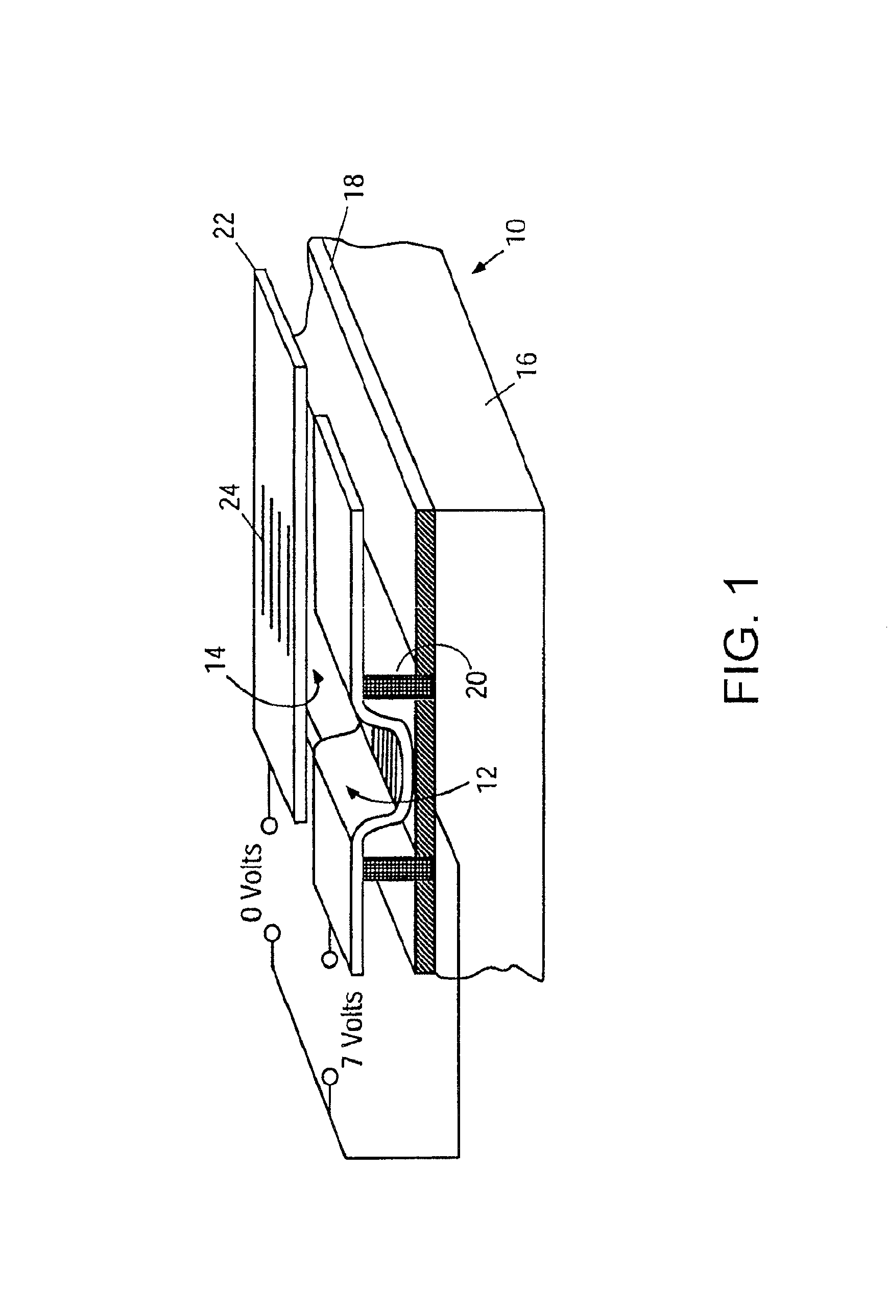
[0008]FIG. 1 of the drawings shows an example of a part of a Visible Spectrum Modulator Array 10 which may be fabricated in accordance with techniques described herein. Referring to FIG. 1, an antenna array i...


PUM

PropertyMeasurementUnit
metallicaaaaaaaaaa
polymericaaaaaaaaaa
conductiveaaaaaaaaaa

Abstract

The invention provides a microfabrication process which may be used to manufacture a MEMS device. In one embodiment, the process comprises depositing at least one first layer on a substrate. The process further comprises patterning said first layer to define at least a first portion of said microelectromechanical system device. The process further comprises depositing a second layer on said first layer. The process further comprises patterning said second layer using said first layer as a photomask. The process further comprises developing said second layer to define at least a second portion of the microelectromechanical system device.

Description

RELATED APPLICATIONS[0001]This application is a continuation of U.S. patent application Ser. No. 10 / 074,562, filed Feb. 12, 2002 now U.S. Pat. No. 6,794,119, which is incorporated by reference in its entirety.FIELD OF THE INVENTION[0002]This invention relates to microfabrication. In particular, it relates to the microfabrication of a structure for a Microelectromechanical Systems (MEMS) device.BACKGROUND[0003]Microfabrication techniques used to fabricate MEMS devices generally involve the deposition of one or more layers on a substrate and the subsequent patterning of the layers to produce useful structures. One technique for patterning a layer involves the use of photolithography. With photolithography a photographic definition of a desired pattern on a photo or optical mask is used to impart the pattern onto a surface of the layer. When manufacturing a MEMS device usually several masking steps are required, each masking step adding to the cost of the device. Accordingly, it is des...

Claims


Application Information

Patent Timeline
Patent Type & Authority Patents(United States)
IPC IPC(8): H01L21/00G02B26/08B81B3/00B81C1/00G02B26/00G03F7/20
CPCB81C1/00396G02B26/001B81B2201/042B81B2203/0315B81C2201/0109B81C2203/0136B81C1/00G03F7/00G03F7/20B81B7/02
Inventor MILES, MARK W.
Owner SNAPTRACK
Why Eureka
Try Eureka