High performance vias for vertical IC packaging

a vertical packaging and via technology, applied in the direction of electrical equipment, semiconductor devices, semiconductor/solid-state device details, etc., can solve the problems of high cost of particular hand labor, high cost of prior vertical packaging techniques, and largely eluded or otherwise resisted assembly automation and any incorporation into the regular wafer fabrication context. , to achieve the effect of low cos

Inactive Publication Date: 2005-08-30
NORTHROP GRUMMAN SYST CORP
View PDF8 Cites 83 Cited by
  • Summary
  • Abstract
  • Description
  • Claims
  • Application Information

AI Technical Summary

Benefits of technology

[0007]A plurality of the semiconductor dies or similarly constructed semiconductor chip scale substrates are stacked on one another with the metal bonding pad of one substrate of the stack located opposite the via hole in an adjacent substrate of the stack and with the solder bump on the metal bonding pad of the one substrate soldered to the via of the adjacent substrate. The outer end of the solder bump on the one substrate extends within the via hole in the adjacent substrate. Surface tension forces during reflow soldering are effective to finely align the substrates during soldering. According to the method of making the stack of a plurality of semiconductor chip scale substrates of the invention, the chip scale substrates are semiconductor wafers wherein after the stacking and reflow soldering, the soldered wafers are diced to form a plurality of stacks of semiconductor dies. The invention enables a vertical interconnection / packaging which can be completely automated using existing wafer processing and automated assembly equipment and thus achieves state-of-the-art reproducibility, consistency, quality and low cost.

Problems solved by technology

This technique, which is particularly hand labor intensive is expensive.
Prior vertical packaging techniques have largely eluded or otherwise resisted assembly automation and any incorporation into the regular wafer fabrication context.
Thus, products of these prior techniques have been very expensive, and quality / consistency challenged and, in the case of memory chips, frequently overtaken in capacity by the next generation chips.
And now, the packing density of memory chips will reach its limit known in the art where devices can be made so small that they no longer exhibit useful behavior.

Method used


Image

  • High performance vias for vertical IC packaging
  • High performance vias for vertical IC packaging
  • High performance vias for vertical IC packaging

Examples


Embodiment Construction

[0013]In the following detailed description, like reference numerals and characters may be used to designate identical, corresponding, or similar components in differing drawing figures. Furthermore, in the detailed description to follow, example sizes / models / values / ranges may be given, although the present invention is not limited thereto. Well-known power connections and other well-known elements have not been shown within the drawing figures for simplicity of illustration and discussion and so as not to obscure the invention.

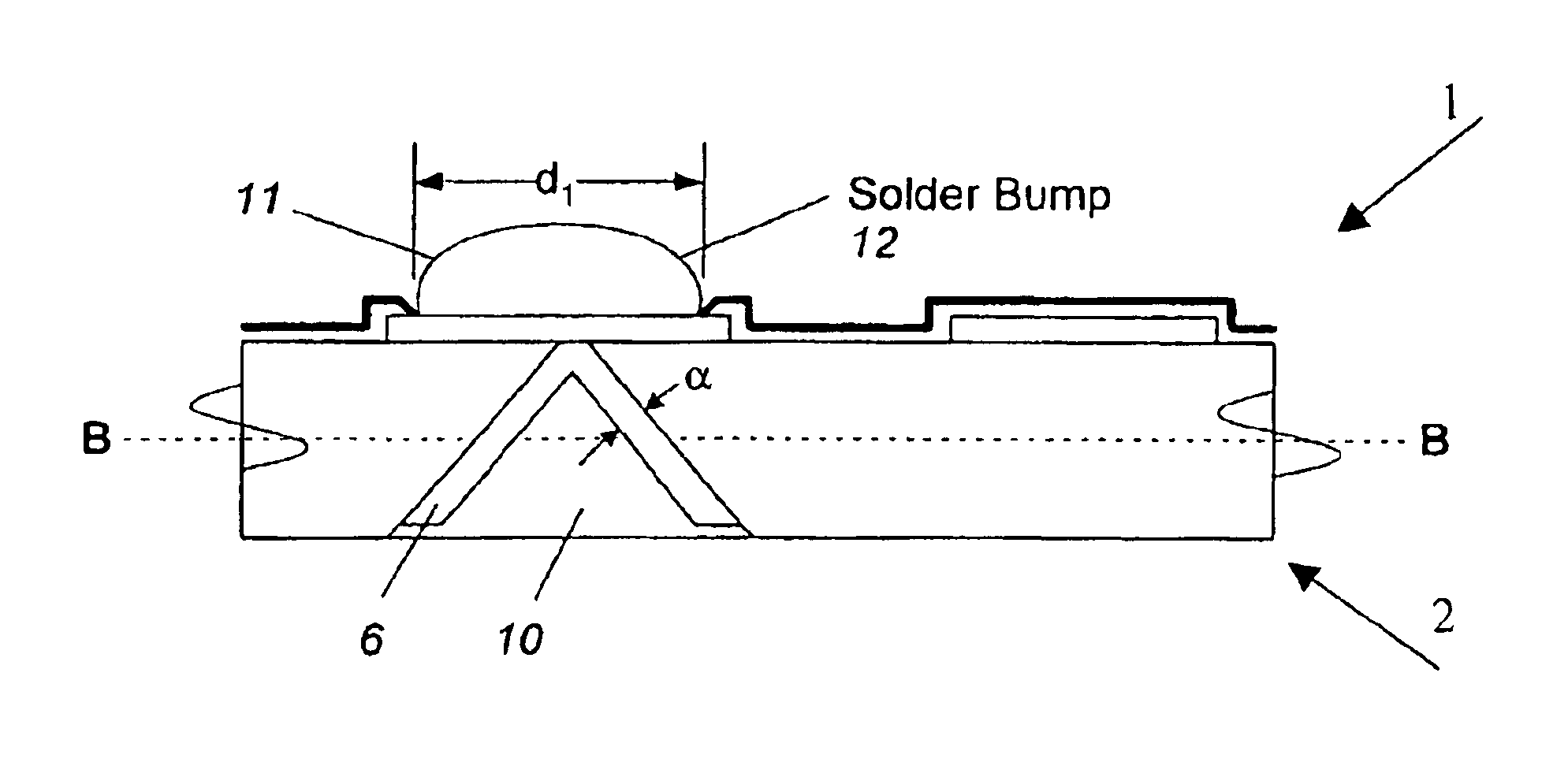
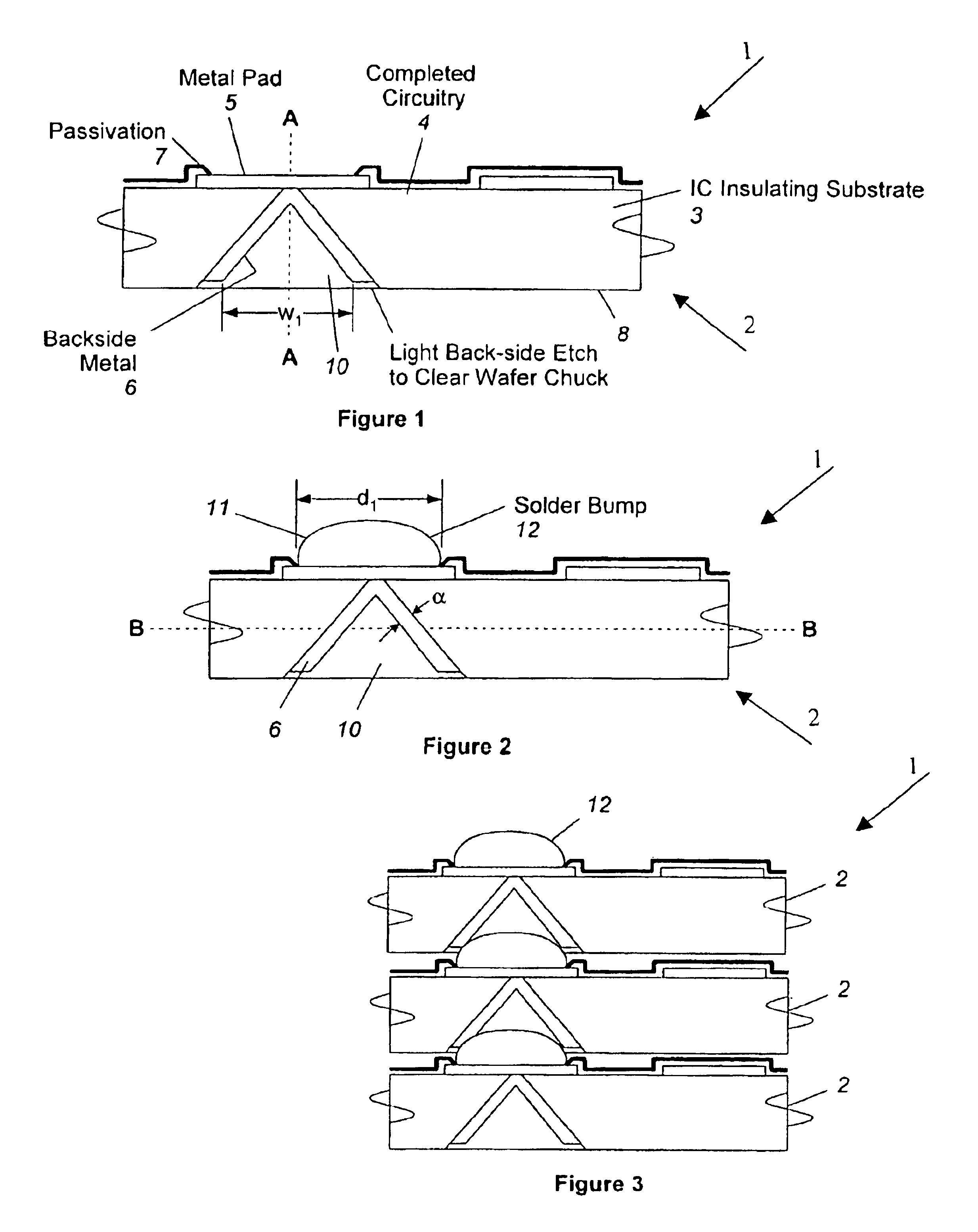
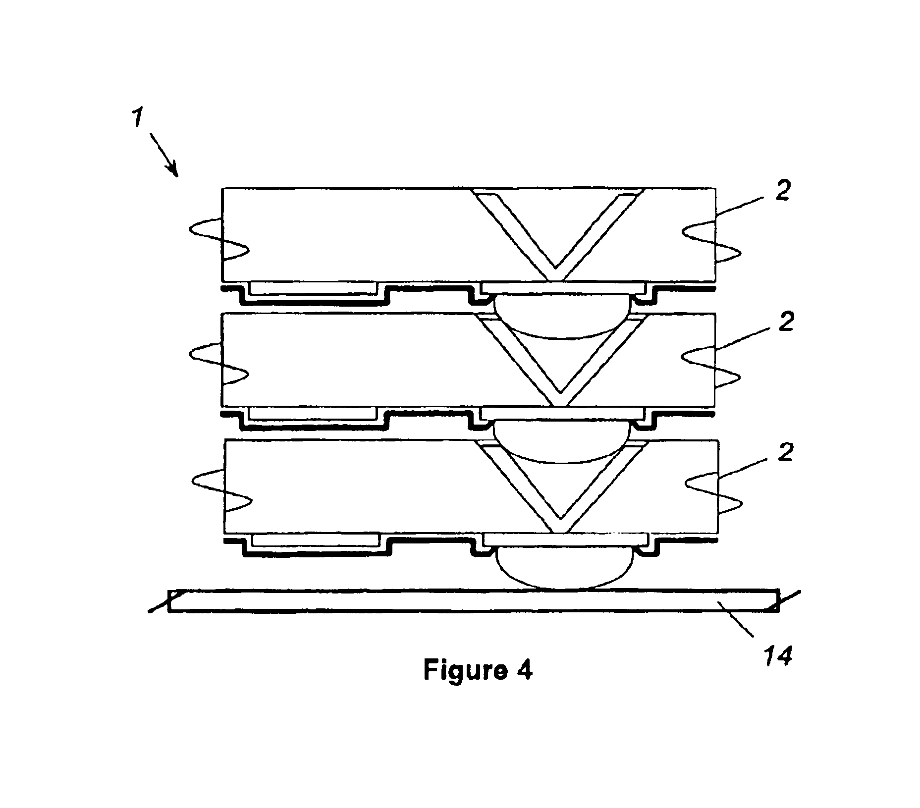
[0014]Referring now to the drawings, a semiconductor device 1 according to the present invention comprises a semiconductor die 2 having an insulating substrate 3 with integrated circuitry 4 formed on a front side of the substrate. A metal bonding pad 5 overlies the substrate on the front side thereof and is electrically connected to the integrated circuitry. A passivation 7 is provided over the front side of the substrate about the metal bonding pad. An elect...


PUM


Abstract

A semiconductor device, a microelectromechanical system package and a method of making the same utilize high performance vias for vertical IC packaging. A semiconductor die of the device / package has a substrate with integrated circuitry formed on a front side of the substrate. A metal bonding pad overlies the substrate on the front side of the substrate and is electrically connected to the integrated circuitry. A solder bump is located on the metal bonding pad. An electrically conductive via extends through the substrate from the metal bonding pad to a back side of the substrate where the via forms a side wall of a via hole. A plurality of the substrates are stacked on one another with the outer end of the solder bump of one substrate fitting within the via hole of an adjacent substrate. During reflow soldering, surface tension forces of the molten solder bump self-align the substrates.

Description

BACKGROUND OF THE INVENTION[0001]1. Field of the Invention[0002]A semiconductor device and a microelectromechanical system package and a method of making the same involve vertically packaging and simultaneously electrically interconnecting a plurality of semiconductor chip scale substrates using high performance vias.[0003]2. Discussion of the Related Art[0004]Prior vertical packaging techniques require forming an integrated circuit (IC) stack with epoxy followed by mechanically lapping the sides of this formation in preparation for forming the interconnect between the IC's in the stack along these sides of the stack. Prior techniques require the formation and attachment of lead frames to each die in order to bring what would have been bonding pads out to the edges of the stack. Some prior techniques employ conductive epoxy for signal and power traces along the sides of the stack. This technique, which is particularly hand labor intensive is expensive.[0005]Prior vertical packaging ...

Claims


Application Information

Patent Timeline
Patent Type & Authority Patents(United States)
IPC IPC(8): H01L25/065H01L23/48H01L23/52H01L21/3205H01L21/60H01L25/07H01L25/18
CPCH01L23/481H01L25/0657H01L2224/16237H01L2225/06517H01L2225/06541H01L2225/06555H01L2225/06589H01L2224/16147H01L2224/81141H01L2224/05573H01L2224/056H01L2924/00014
Inventor AKERLING, GERSHONANDERSON, JAMES M.UPTON, ERIC L.
Owner NORTHROP GRUMMAN SYST CORP
Why Eureka
Try Eureka