

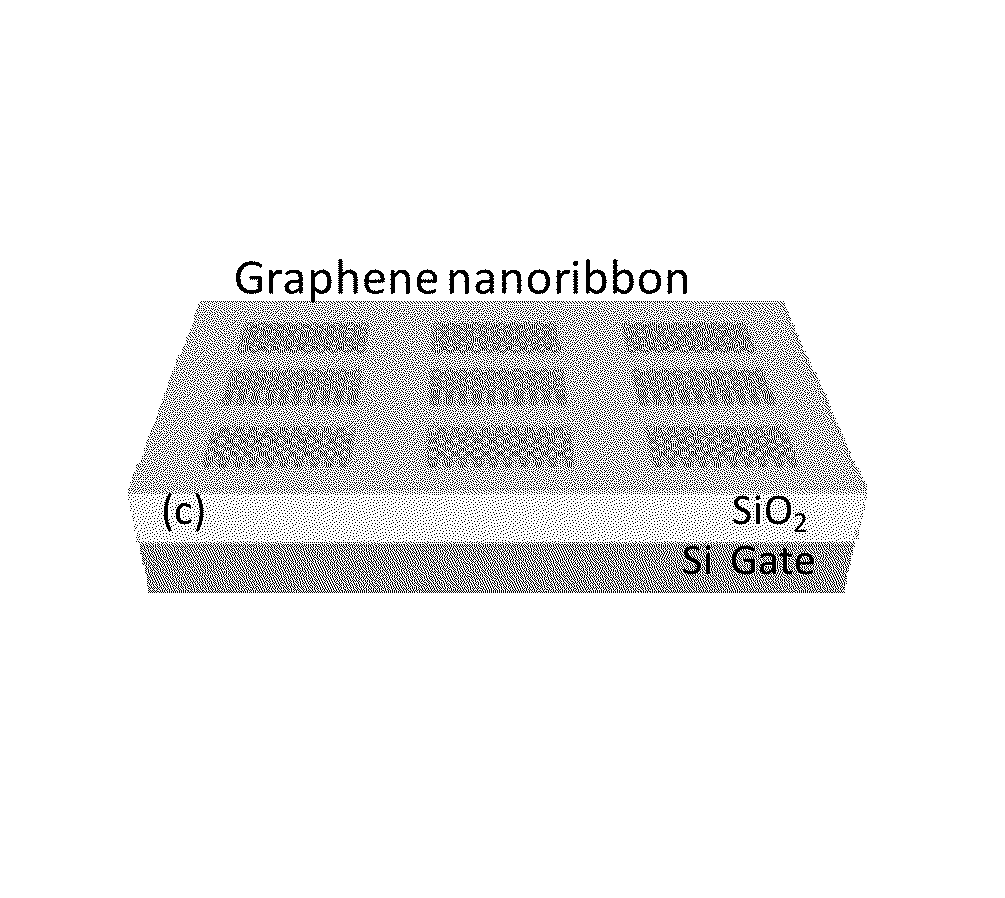
Silicon-graphene waveguide photodetectors, optically active elements and microelectromechanical devices
a waveguide photodetector and waveguide technology, applied in the field of photodetectors, optical modulators and micromechanical devices, can solve the problems of high cost of optical devices, complexity and cost of electronics, and the limited free-carrier diffusion speed of the fastest commercially available optical detectors and modulators available today, so as to improve the optical field strength
- Summary
- Abstract
- Description
- Claims
- Application Information
AI Technical Summary
Benefits of technology
Problems solved by technology
Method used
Image

Examples
Embodiment Construction
[0080]We now describe high index contrast waveguides that are useful to concentrate light in order to enhance nonlinear optical effects in various materials so that such effects can be employed to manipulate light (or more generally electromagnetic radiation) at low power levels, as compared to conventional systems and methods that employ nonlinear optical materials. The manipulation of electromagnetic radiation or light can be useful to provide a variety of components that perform operations on light such as rectification, modulation, filtering, and logic operations in a manner analogous to the same operations which are provided using electronic devices operating on electrical signals. For example, an input a light wave to be processed is impressed onto the component. The light wave has at least one parameter characterizing the light wave, such as one of an intensity, a polarization, a frequency, a wavelength, and a duration (e.g., a pulse length, or in the case of continuous wave ...
PUM
 Abstract
Description
Claims
Application Information