Image sensor and method for fabricating the same

a technology of image sensor and manufacturing method, which is applied in the field of image sensor, can solve the problem of rare improvement of image sensor efficiency, and achieve the effect of preventing the brightness and resolution of captured images from being reduced

Inactive Publication Date: 2007-08-07
SHINILL KANG +1
View PDF11 Cites 33 Cited by
  • Summary
  • Abstract
  • Description
  • Claims
  • Application Information

AI Technical Summary

Benefits of technology

[0033]An object of the present invention is to change a structure of an image sensor to prevent brightness and resolution of captured images from being reduced because amounts of light sensed by photoelectric elements are small in some positions in the image sensor.
[0034]That is, the object of the present invention is to improve efficiency of the image sensor by making very intensive and homogeneous light sensed in every position in the image sensor, when light from a lens system passes through a color filter layer of a substrate and is sensed by the photoelectric elements.
[0035]The present invention takes notice of radical reasons of problems of the conventional image sensor, and solves the problems to raise efficiency of the image sensor. The conventional methods stick to resultant phenomena rather than radical countermeasures, and thus rarely improve efficiency of the image sensor. However, the present invention can considerably improve efficiency of the image sensor.

Problems solved by technology

The conventional methods stick to resultant phenomena rather than radical countermeasures, and thus rarely improve efficiency of the image sensor.

Method used


Image

  • Image sensor and method for fabricating the same
  • Image sensor and method for fabricating the same
  • Image sensor and method for fabricating the same

Examples


Embodiment Construction

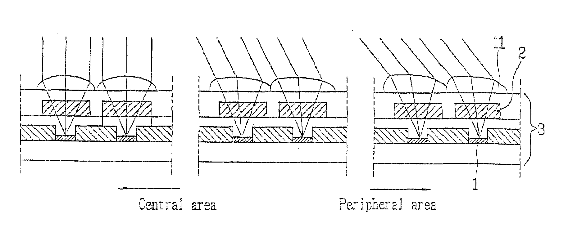
[0076]An image sensor and a method for fabricating the same in accordance with preferred embodiments of the present invention will now be described in detail with reference to the accompanying drawings.

[0077]FIG. 8 is a concept view showing that a prism 10 can vary an optical path of light.

[0078]As illustrated in FIG. 8, the micro prism 10 converts the optical path of light to be parallel to an optical axis in order to prevent reduction of optical efficiency due to light slantingly incident on peripheral pixels of an image sensor.

[0079]The relations between an inclination angle of light incident on the surface of the prism 10, an angle of refracted light and a gradient value of an incident surface of the prism 10 will now be explained with reference to FIG. 9.

[0080]FIG. 9 illustrates the refraction law of light, especially light passing through the prism 8 of FIG. 8.

[0081]FIG. 9 shows a refraction path of light when light is incident on an interface between different media having a ...


PUM


Abstract

An image sensor includes a substrate in which photoelectric elements have been formed, and an array of optical path conversion elements formed at a light so that the optical path converted light may be incident on the substrate, wherein each of the optical path conversion elements has different tangent line gradients on the corresponding parts of incident surfaces according to distances from the center of the image sensor in order to compensate for differences of incident angles of incident light according to the distances from the center of the image sensor. In addition, a method for fabricating the image sensor fabricates the optical path conversion elements according to a photolithography process using a gray scale mask, combinations of the photolithography process and a reactive ion etching process, or combinations of the photolithography process, the reactive ion etching process, and an UV-molding process.

Description

CROSS-REFERENCE TO RELATED PATENT APPLICATION[0001]This application claims the benefit of Korean Patent Application No. 2003-0049859, filed on Jul. 21, 2003, in the Korean Intellectual Property Office and International Application No. PCT / KR2004 / 000729, filed on Mar. 30, 2004, the disclosures of which are incorporated herein in their entirety by reference.[0002]1. Field of the Invention[0003]The present invention relates to an image sensor and a method for fabricating the same, and more particularly to, an image sensor and a method for fabricating the same, which can make intensive and homogeneous light sensed in every position of the image sensor.[0004]2. Description of the Related Art[0005]An image sensor such as a CCD or CMOS has been used for various products including a digital camera, a digital camcorder, a CCTV, etc. The image sensor is used together with lenses in order to improve performance of the products. There have been increasing demands of consumers on high performanc...

Claims


Application Information

Patent Timeline
Patent Type & Authority Patents(United States)
IPC IPC(8): H01J3/14H01L27/00H01L27/146H01L31/0216H01L31/0232H01L31/10
CPCH01L27/14621H01L27/14625H01L27/14627H01L27/14629H01L31/02162H01L31/0232H01L27/14685H01L27/14605H01L31/02327H01L27/146
Inventor KANG, SHINILL
Owner SHINILL KANG
Why Eureka
Try Eureka