Neutralization techniques for differential low noise amplifiers

a low-noise amplifier and neutralization technology, applied in the field of differential low-noise amplifiers, can solve the problems of inconvenient lna application, inconvenient lna application of basic (lower frequency) amplifier configuration and techniques, and inability to adapt to high-frequency applications, so as to improve input-output isolation without reducing available voltage headroom

Inactive Publication Date: 2007-08-14
SEIKO EPSON CORP
View PDF4 Cites 47 Cited by
  • Summary
  • Abstract
  • Description
  • Claims
  • Application Information

AI Technical Summary

Benefits of technology

[0024]It is an object to provide an LNA circuit suitable for IC applications that provides improved input-output isolation without reducing available voltage headroom as compared to a classical LNA.
[0027]The present invention neutralizes this feedback Cgd capacitance by providing a variable capacitive source, i.e. a variable capacitor, coupled between the control gate of an LNA's first input MOS transistor to the drain of the LNA's second input MOS transistor. The variable capacitor tracks the Cgd of the first input MOS transistor, but is little affected the gate-to-source capacitance of the first input MOS transistor. In this manner it can more closely match the feedback Cdg capacitance, alone, of the first input MOS transistor. Furthermore, since a change in potential difference between the source and drain of the of the first MOS transistor can also affect the amount of feedback current through the first MOS transistor's Cgd capacitance, the present variable capacitor is also made to limit current in a similar manner.
[0032]Furthermore, the general voltage difference across the drain and source of the first input MOS transistor is reproduced across the source and drain of the first neutralizing MOS transistor. This further aids in appropriately sizing the compensating current to more closely match the feedback current through the Cgd of the first input MOS transistor.

Problems solved by technology

The input impedance requirement places practical limitations on the physical configuration of an LNA-type amplifier.
That is, basic (lower frequency) amplifier configurations and techniques may not be suitable for LNA applications.
This approach is indeed suitable for many lower frequency applications, but it is ill-suited for high frequency applications (i.e. at which LNA-type amplifier are typically used).
These two effects generally result in unacceptable noise figures, which make the use of a physical input resistor unsuitable for high-frequency, low-power applications, and thus unsuitable for LNA-type amplifiers.
Therefore, attempting to use the control gate as the input to an MOS transistor to provide an ohmic (not capacitive) input impedance (such as a matching 50Ω input resistance) without adding a physical resistor (to avoid the noise characteristics of physical resistors) may appear to be a futile endeavor.
However, this approach affects the overall performance of the transistor.
However, LNA-type amplifiers are typically used in narrow band applications, so this narrow-band operation limitation is typically not critical a hindrance.
The value of Ls needed to produce the desired input resistance, however, may not necessarily be at resonance at the desired operating frequency of the LNA.
LNA-type amplifiers, however, typically do not have the simplified structures of FIGS. 4 and 5.
Other methods of compensating for, or neutralizing, the Miller effect are known, but are not considered suitable for modern LNA applications.
But this approach is unsuited for integrated circuit, IC, implementation due to the large area requirements and poor quality of integrated tapped transformers.
However, since the Cgd of an MOS transistor is voltage-dependent (i.e. it varies with an applied potential) precise matching with the feedback capacitor has not been realizable.
Therefore, this technique has traditionally had only limited application in semiconductor amplifiers.
This difficulty in matching capacitances is particularly important in LNA amplifiers, where a mismatch in the feedback capacitor could set-up a separate resonance through the feedback capacitor leading to instabilities.
Consequently, this approach has traditionally been limited to vacuum tube technology, which have highly linear and relatively constant coupling capacitances.

Method used


Image

  • Neutralization techniques for differential low noise amplifiers
  • Neutralization techniques for differential low noise amplifiers
  • Neutralization techniques for differential low noise amplifiers

Examples


Embodiment Construction

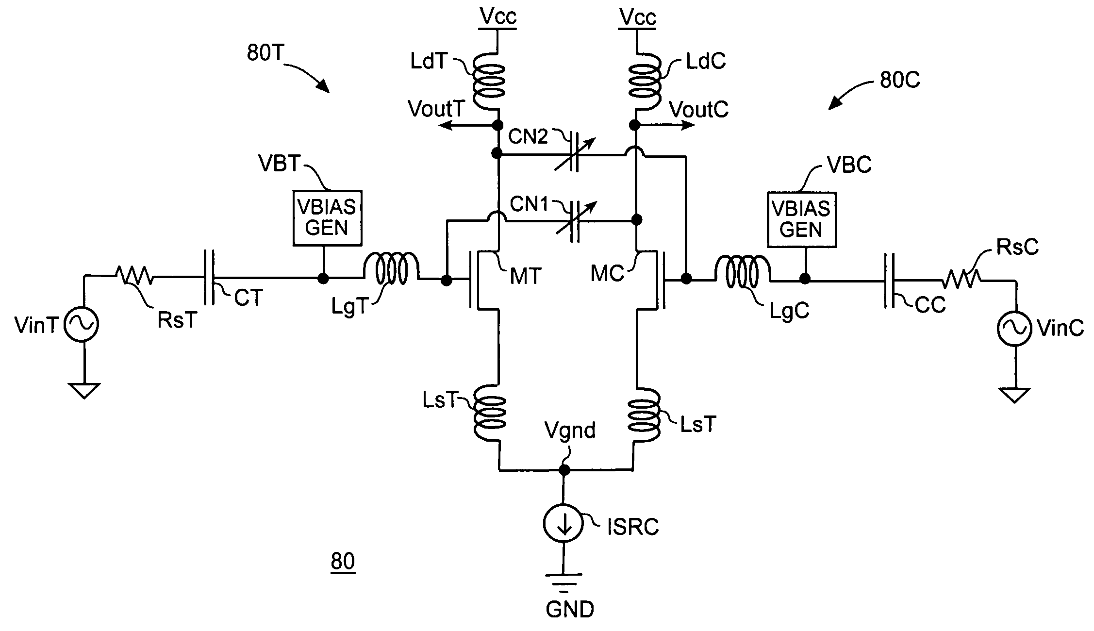
[0046]With reference to FIG. 8, a differential low noise amplifier, LNA, 80 in accord with the present invention includes a true branch 80T and a complementary branch 80C. The true branch 80T of LNA 80 includes a first (true) transistor MT for receiving a true signal, a first gate inductance LgT coupled to the control gate of MT, a first source inductance LsT coupling the source node of MT to a virtual ground node Vgnd, a first drain inductance LdT coupling the drain of MT to Vcc, a first voltage bias generator VBT, a first input coupling capacitor CT, a first input signal VinT, and the first input signal's corresponding source impedance RsT.

[0047]In the present case, true and complementary transistors MT and MC, are implemented as metal oxide semiconductor, MOS, transistors, but it is to be understood that true and complementary transistors MT and MC may be implemented as bipolar junction transistors, junction field transistors or other known field effect transistors.

[0048]The comp...


PUM


Abstract

An differential LNA has first and second input MOS transistors, with differential inputs applied to their respective control gates and differential outputs taken at their respective drains. The gate-to-drain, Cgd, feedback capacitances of the first and second input MOS transistors are neutralized by respective gate-to-source, Cgs, capacitances in the two neutralizing MOS transistors. A first neutralizing MOS transistor has its control gate coupled to the control gate of the first input MOS transistor, its source node coupled to the drain node of the second input MOS transistor, and its drain node coupled to a fixed potential. A second neutralizing MOS transistor has its control gate coupled to the control gate of the second input MOS transistor, its source node coupled to the drain node of the first input MOS transistor, and its drain node coupled to the same fixed potential. In this manner, similar and opposite potential differences between the gate-and-drain and the drain-and-source regions of the first input MOS transistor are reproduced in gate-and-drain and drain-and-source regions of the first neutralizing MOS transistor. A similar affect is produced in the second input and second neutralizing MOS transistor.

Description

BACKGROUND OF THE INVENTION[0001]1. Field of the Invention[0002]The present invention relates to the field of differential low noise amplifiers, LNA. Specifically, the present invention relates to improving input-output isolation in an LNA.[0003]2. Description of the Related Art[0004]The first stage of a high frequency receiver is typically a low-noise amplifier, LNA. The LNA is particularly a key component in wireless communication applications. In such systems, LNAs are used to receive and amplify a signal from an antenna without adding significant noise to the receiver. In addition to amplifying a received signal, typically the LNA is also required to provide a specific input impedance at a prescribed operating frequency. This impedance requirement is particularly important since the impedance quality can greatly affect the performance of passive filters that may precede the LNA. Overall the LNA is one of the most important circuit blocks in a receiver chain for determining the n...

Claims


Application Information

Patent Timeline
Patent Type & Authority Patents(United States)
IPC IPC(8): G06G7/12H03F3/45
CPCH03F1/14H03F1/26H03F3/191H03F3/45183H03F2200/294H03F2200/372H03F2203/45332H03F2203/45366H03F2203/45464H03F2203/45544H03F2203/45608H03F2203/45622H03F2203/45638
Inventor EID, SALEMBLUM, GREGORY A.
Owner SEIKO EPSON CORP
Why Eureka
Try Eureka