Methods and devices for connecting and grounding an EMI shield to a printed circuit board

a technology of electromagnetic interference and printed circuit board, which is applied in the direction of electrical apparatus construction details, coupling device connections, localised screening, etc., can solve the problems of increasing the cost of electronic equipment, cellular phones, and existing solutions

Active Publication Date: 2007-08-21
WAVEZERO +1
View PDF15 Cites 46 Cited by
  • Summary
  • Abstract
  • Description
  • Claims
  • Application Information

AI Technical Summary

Benefits of technology

[0020]In yet another embodiment, the connector comprises one or more conductive mechanical clips that are fixedly coupled to at least a portion of the ground trace of the printed circuit board with a conductive adhesive or solder. The mechanical clips may releasably couple the EMI shield to a grounding portion of the printed circuit board (e.g., a ground trace) so as to allow for easy removal of the EMI shield from the grounding portion. In one configuration, the conducive mechanical clips comprise a body that has first and second opposing arms. A portion of the EMI shield, such as the flange or sidewall, is received between the first and second arms and are mechanically and electrically coupled to the grounding portion of the printed circuit board.

Problems solved by technology

In virtually all cases, however, the existing solutions are expensive and add significant costs to providing electronic equipment such as cellular phones, personal digital assistants (PDA), laptop computers, set-top boxes, cable modems, networking equipment including switches, bridges, and cross-connects, among a multitude of other electronic products.
However, since a polymer substrate is used to create these types of EMI shields, some of the common methods used to attach and locate more traditional, metal EMI shielding solutions onto a printed circuit board are not applicable for polymer based shields.
However, if this same solder technique is used in conjunction with a metallized plastic shield, the heat from the molten solder would damage the plastic substrate and potentially compromise the shielding effectiveness of the EMI shield.

Method used


Image

  • Methods and devices for connecting and grounding an EMI shield to a printed circuit board
  • Methods and devices for connecting and grounding an EMI shield to a printed circuit board
  • Methods and devices for connecting and grounding an EMI shield to a printed circuit board

Examples


Embodiment Construction

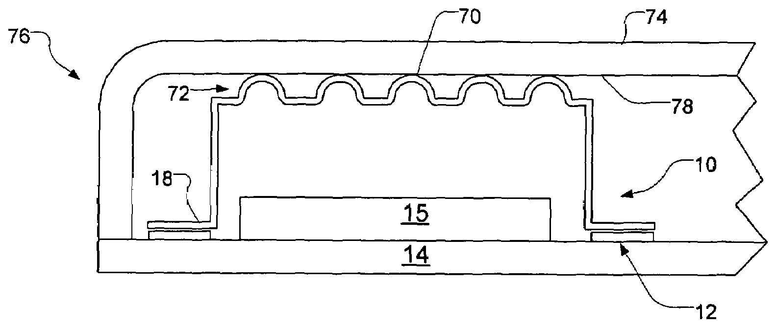
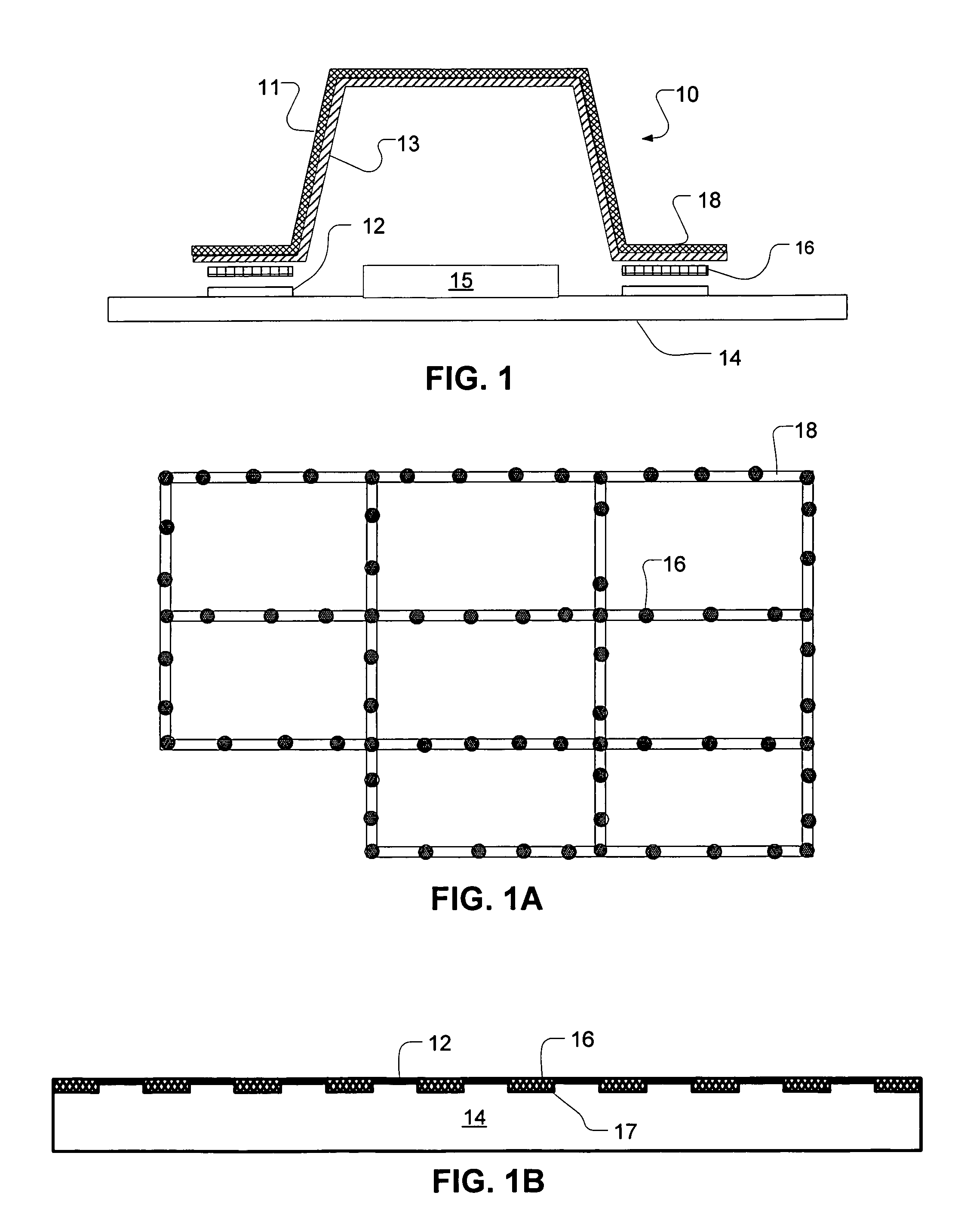
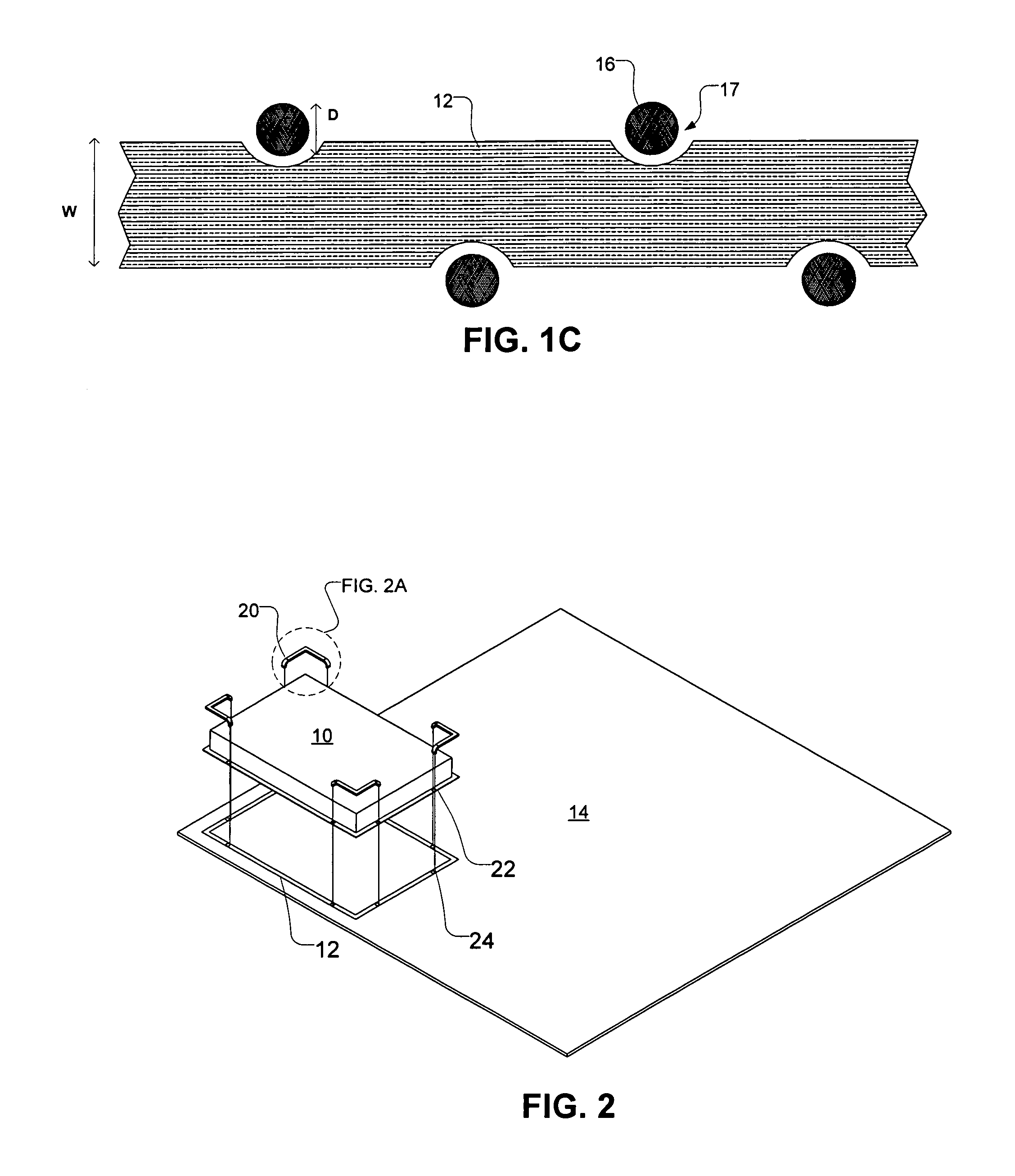
[0054]The present invention provides methods and assemblies for connecting and grounding an electromagnetic interference (EMI) shield to a printed circuit board (PCB) of an electronic device.

[0055]The EMI shields of the present invention typically include a resin film layer that can be formed by a variety of plastic processing methods to a desired shape to partially or fully enclose a printed circuit board and the electronic components on the printed circuit board. In exemplary embodiments, the resin film layer is a thermoformable plastic that is shaped using thermoforming techniques (e.g., vacuum, pressure, or mechanical forces). It should be appreciated however, that the resin film layer can be shaped using any conventional or proprietary methods. The resin film layer of the EMI shield typically has at least one metal layer on at least one side of the resin film layer. The metal layers will have a thickness that is sufficient to block the transmission of EMI, typically between abo...


PUM


Abstract

The present invention provides electronic devices, kits, and connector assemblies for coupling an EMI shield to a ground trace. In one embodiment, the present invention provides an electronic device comprising a printed circuit board and an EMI shield that has a flange around at least a portion of a perimeter of the EMI shield. One or more connectors coupled to the flange removably contact the flange to a ground trace of the printed circuit board.

Description

CROSS-REFERENCES TO RELATED APPLICATIONS[0001]The present application claims benefit to U.S. Provisional Patent Application Ser. No. 60 / 449,934, filed Feb. 26, 2003 and U.S. Provisional Patent Application Ser. No. 60 / 452,678, filed Mar. 10, 2003, the complete disclosures of which are incorporated herein by reference.BACKGROUND OF THE INVENTION[0002]The present invention relates generally to methods of connecting an electromagnetic interference (EMI) shield to a printed circuit board (PCB) of an electronic device. In particular, the present invention relates to different shield design techniques, features and the use of secondary connector components to efficiently and effectively connect one or more EMI shields to a printed circuit board.[0003]All electronic products emit electromagnetic radiation, generally in the range of 50 MHz to 3 GHz, but not limited to this range, especially considering the recent advances in high-speed microprocessor design and the rapidly increasing capabil...

Claims


Application Information

Patent Timeline
Patent Type & Authority Patents(United States)
IPC IPC(8): H05K7/14H05KH05K9/00
CPCH01R23/6873H05K9/003H01R13/6595
Inventor ZARGANIS, JOHNARNOLD, ROCKY R.
Owner WAVEZERO
Why Eureka
Try Eureka