Semiconductor heating apparatus

a heating apparatus and semiconductor technology, applied in the direction of heater elements, semiconductor/solid-state device testing/measurement, instruments, etc., can solve the problems of low thermal capacity, difficult to maintain, and difficult to raise and lower the temperature of the heater, so as to achieve low thermal capacity, low cost, and high rigidity.

Inactive Publication Date: 2007-09-11
SUMITOMO ELECTRIC IND LTD
View PDF11 Cites 30 Cited by
  • Summary
  • Abstract
  • Description
  • Claims
  • Application Information

AI Technical Summary

Benefits of technology

[0008]The object of the invention is to solve the above problems. In other words, the object of the present invention is to provide a semiconductor heating apparatus, in which, when measuring the electrical properties of multiple chips formed on a large wafer, one or several chips are heated uniformly, and the other chips are on standby at a low temperature. A further object of the present invention is to provide a semiconductor heating apparatus which has high rigidity, low thermal capacity, with little likelihood of warping, and a metal layer with sufficiently low electrical resistance.

Problems solved by technology

If the heater is thin, the heater can become deformed, and there may be contact failure between the wafer and the ground electrode.
Raising and lowering the temperature of the heater requires a long time, and this has become a major obstacle in improving throughput.
Even though it is thin, the ceramic substrate has high rigidity and does not deform readily.
As a result, this wafer prober does not readily deform and has a small thermal capacity.
When a chip is exposed to high temperatures for a long period of time, there can be deterioration of properties due to the heat.
However, with the heater of the prior art described above, when a plurality of 20 mm square chips are formed on wafers of diameter 200 mm or 300 mm, it is difficult to raise the temperature of a single chip independently.
In addition, with the self-generated heat as describe above, not only is that chip damaged, but the surrounding chips may be damaged as well.

Method used


Image

  • Semiconductor heating apparatus
  • Semiconductor heating apparatus
  • Semiconductor heating apparatus

Examples


embodiment 1

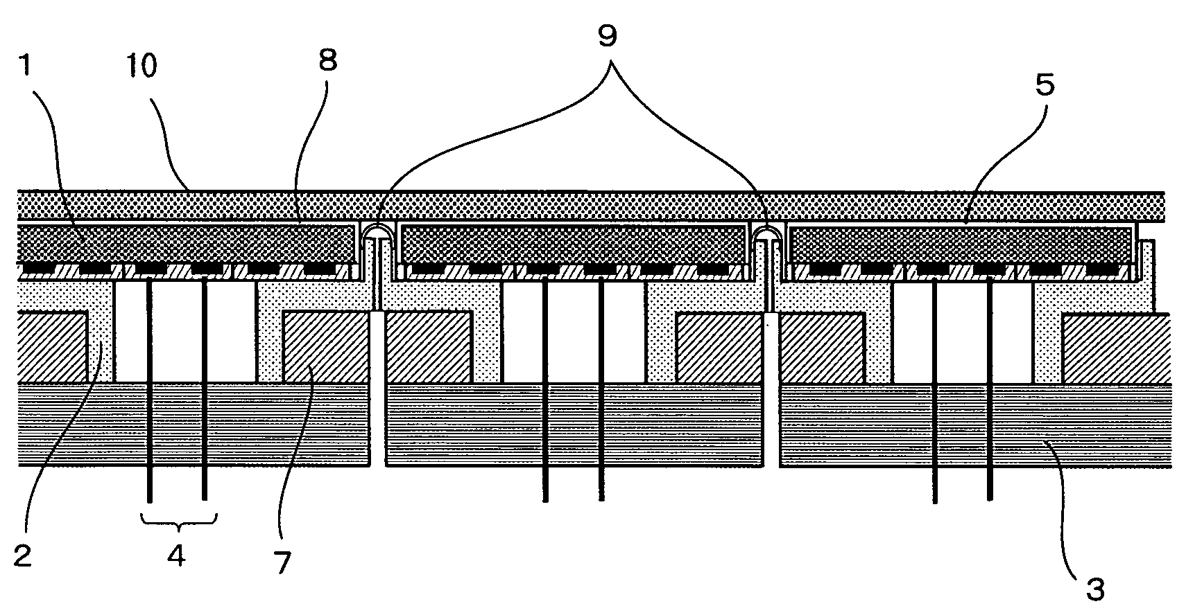
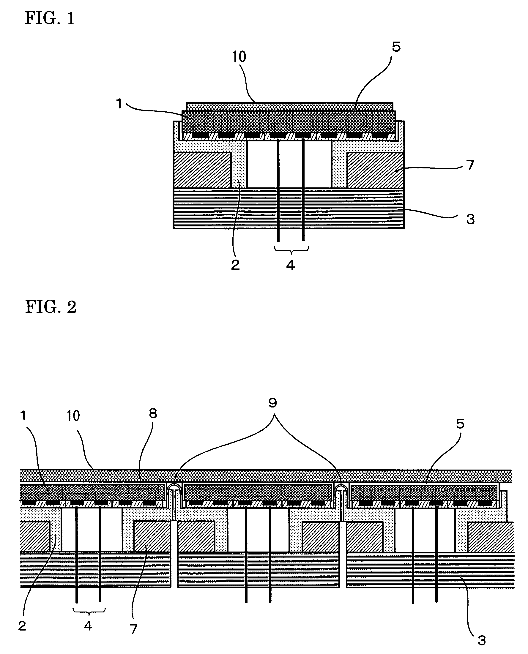
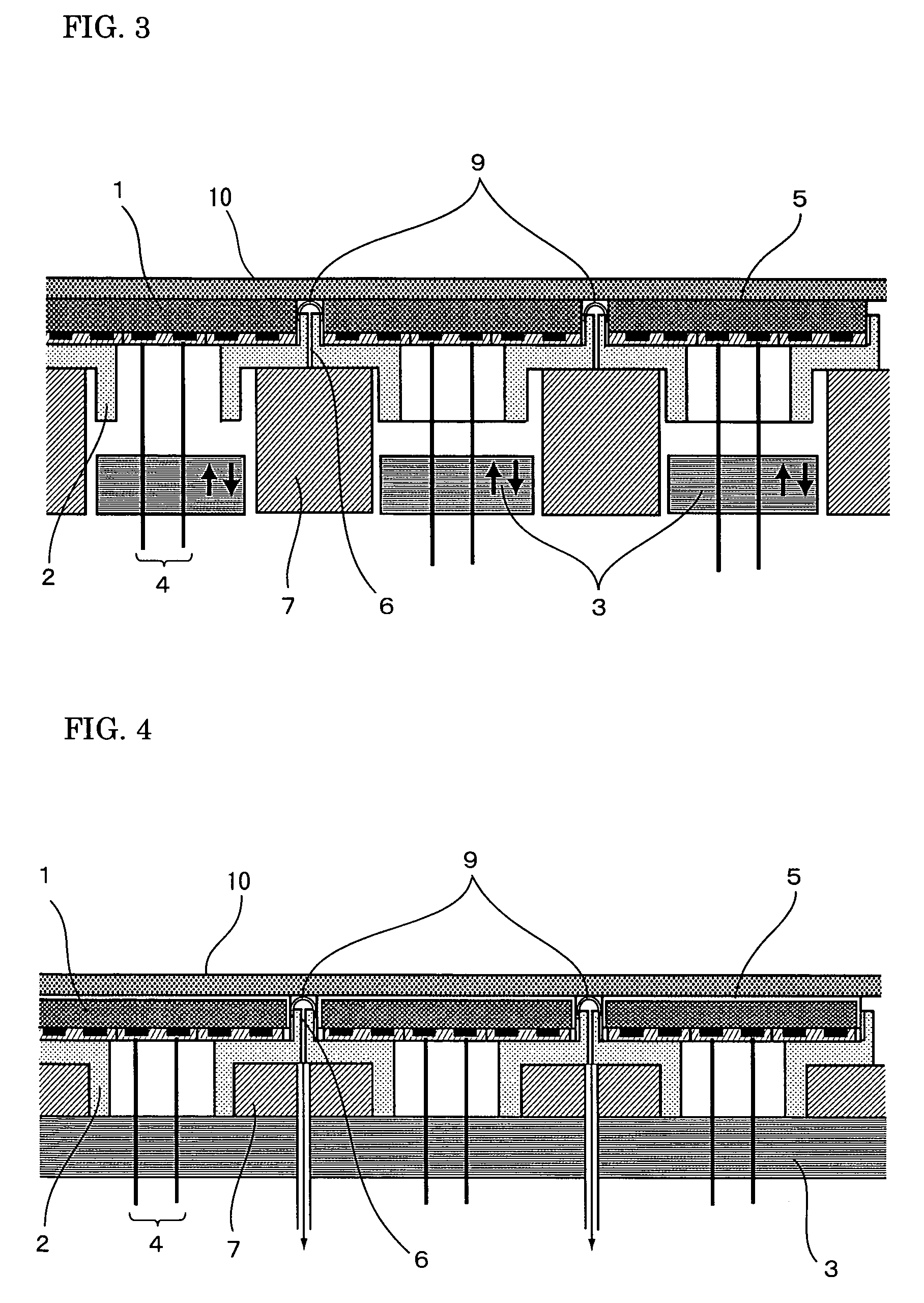
[0040]100 parts by weight of aluminum nitride (AlN) powder and 0.5 parts by weight of yttrium oxide (Y2O3) powder were mixed. Polyvinyl butyral as a binder and dibutyl phthalate as a solvent were mixed at 10 parts by weight and 5 parts by weight, respectively. Granules were created by spray drying. After sintering and then polishing, these were press molded to obtain 32 sintered bodies the size of 38 mm×38 mm×2 mm. These were degreased at a temperature of 700 degrees C. in a nitrogen atmosphere, and these were sintered for 5 hours in a nitrogen atmosphere at 1850 degrees C., and 32 AlN sintered bodies were created. These AlN sintered bodies were processed and finished to a size of 38 mm×38 mm×2 mm. The thermal conductivity of the AlN sintered bodies was 175 W / mK.

[0041]On the 38 mm×38 mm surface of the AlN sintered body, the heating element circuit was screen printed using a W paste. The W paste was created by adding glass powder and an ethyl cellulose binder for calcination to W pow...

embodiment 2

[0049]100 parts by weight of SiC powder, 1.0 part by weight of boron carbide (B4C), and 1.0 part by weight of carbon (C) powder were mixed. Polyvinyl butyral as a binder and dibutyl phthalate as a solvent were mixed at 10 parts by weight and 5 parts by weight, respectively. Granules were created by spray drying. After sintering and polishing, these were press molded to obtain 38 mm×38 mm×2 mm sintered bodies. These were degreased at 700 degrees C. in an argon atmosphere. These were sintered for 5 hours at 1920 degrees C. in an argon atmosphere to create 32 SiC sintered bodies. These SiC sintered bodies were processed and completed to be 38 mm×38 mm×2 mm. The thermal conductivity of the SiC sintered bodies was 150 W / mK. As in Embodiment 1, heating circuits were formed on these SiC sintered bodies, and W terminals and Ni electrodes were attached. The SiC heating parts were completed.

[0050]The heating apparatus was completed in the same manner as in Embodiment 1 except for the 32 heati...

embodiment 3

[0051]100 parts by weight of Si3N4 powder, 1.0 part by weight of Y2O3 powder, and 1.0 part by weight of Al2O3 powder were mixed. Polyvinyl butyral as a binder and dibutyl phthalate as a solvent were mixed at 10 parts by weight and 5 parts by weight, respectively. Granules were created by spray drying. After sintering and polishing, these were press molded to obtain 38 mm×38 mm×2 mm sintered bodies. These were degreased at 700 degrees C. in a nitrogen atmosphere. These were sintered for 5 hours at 1650 degrees C. in a nitrogen atmosphere to create 32 Si3N4 sintered bodies. These Si3N4 sintered bodies were processed and completed to be 38 mm×38 mm×2 mm. The thermal conductivity of the Si3N4 sintered bodies was 80 W / mK. As in Embodiment 1, heating circuits were formed on these Si3N4 sintered bodies, and W terminals and Ni electrodes were attached. The Si3N4 heating parts were completed.

[0052]The heating apparatus was completed in the same manner as in Embodiment 1 except for the 32 hea...


PUM

PropertyMeasurementUnit
forceaaaaaaaaaa
thicknessaaaaaaaaaa
diameteraaaaaaaaaa

Abstract

A semiconductor heating apparatus, in which, when measuring the electrical properties of multiple chips formed on a large size wafer, only one or a several chips are heated uniformly, and the other chips are on standby at a low temperature. The semiconductor heating apparatus includes a heating part for mounting and heating the workpiece, a support part which supports the heating part, and a cooling module which contacts the support part. A plurality of heating parts and supporting parts are joined together. The workpiece mounting surfaces of the plurality of heating parts are preferably constructed in the same plane. In addition, there is preferably a thermal insulating material distributed underneath the support part. The heating part is preferably a ceramic heater.

Description

TECHNICAL FIELD[0001]The present invention relates to a semiconductor heating apparatus used in a semiconductor manufacturing device or a semiconductor testing device. In particular, the present relates to a wafer prober or a handler device or the like.BACKGROUND ART[0002]In the prior art, heat treatment of a semiconductor substrate (wafer) as a workpiece is conducted in a testing step for a semiconductor. In other words, the wafer is heated to a higher temperature than the usual usage temperature, and any semiconductor chips which have the possibility of failing are made to fail at an accelerated rate and are removed. This is a burn-in test in order to prevent the occurrence of failure after shipping. In the burn-in step, after forming a semiconductor circuit on the semiconductor wafer and prior to cutting the individual chips, the electrical performance of each chip is measured while the wafer is being heated. Any defective products are removed. With this burn-in step, there is a ...

Claims


Application Information

Patent Timeline
Patent Type & Authority Patents(United States)
IPC IPC(8): H05B3/68C23C16/00G01R31/26G01R31/30H01L21/00H01L21/02H01L21/66H01L21/68H01L21/683H05B3/06H05B3/10H05B3/20H05B3/74
CPCH01L21/67103H01L21/67109
Inventor KUIBIRA, AKIRANAKATA, HIROHIKOSHINMA, KENJI
Owner SUMITOMO ELECTRIC IND LTD
Why Eureka
Try Eureka