Method for analyzing power distribution system and related techniques

a power distribution system and power distribution technology, applied in the direction of electric variable regulation, process and machine control, instruments, etc., can solve the problems of parasitic inductance and parasitic resistance of wiring, inability of power distribution system to transmit external power completely to the chips, and fragile mechanical properties of semiconductor chips

Active Publication Date: 2007-09-11
VIA TECH INC
View PDF2 Cites 14 Cited by
  • Summary
  • Abstract
  • Description
  • Claims
  • Application Information

AI Technical Summary

Problems solved by technology

However, mechanical properties of the semiconductor chips are fragile, and therefore, the semiconductor chips have to be appropriately packed or be adhered to appropriate encapsulated circuit boards to protect the semiconductor chips.
However, in fact, the power wiring has parasitic inductances and parasitic resistances, and there are electrical couplings between the power wiring also.
The properties of the power distribution system for transmitting power are affected by the abovementioned non-ideal factors so that the power distribution system is not able to transmit external power completely to the chips.
However, while the time-variant bias current is transmitted, and while the time-variant bias current flows through the power wiring, the power wiring consumes voltage of the bias current and lowers the transmitted bias voltage because of parasitic equivalent inductances on the power wiring of the power distribution system.
Such non-ideal factors affect other bias operations in the chip and result in errors.
This leads to severe variations of a total bias current of the chip so that the voltage transmitted by the power wiring is lowered more obviously.
For a power distribution system, the non-ideal factors lead to a simultaneous switching noise (SSN) of the bias voltage.
However, the abovementioned analysis methods have defects.
In the power distribution system, except for the equivalent inductance Leff provided from a self-inductance of the wiring of single set of pads, there may also be mutual inductances and parasitic capacitances between the power wiring of various sets of pads, and this affects the properties and the performance of the power distribution system, such as the voltage degradation.
This is not able to concretely point out the effects caused by the mutual inductances and not able to precisely estimate the performance of the power distribution system.

Method used


Image

  • Method for analyzing power distribution system and related techniques
  • Method for analyzing power distribution system and related techniques
  • Method for analyzing power distribution system and related techniques

Examples


Embodiment Construction

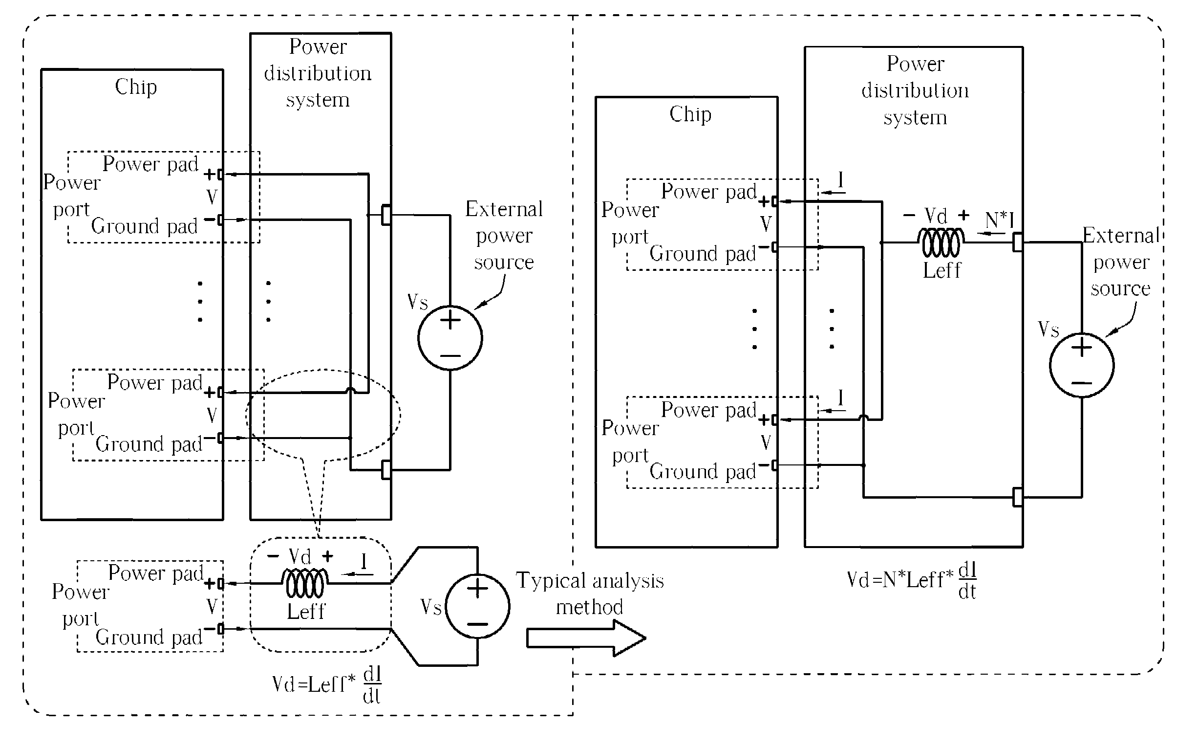
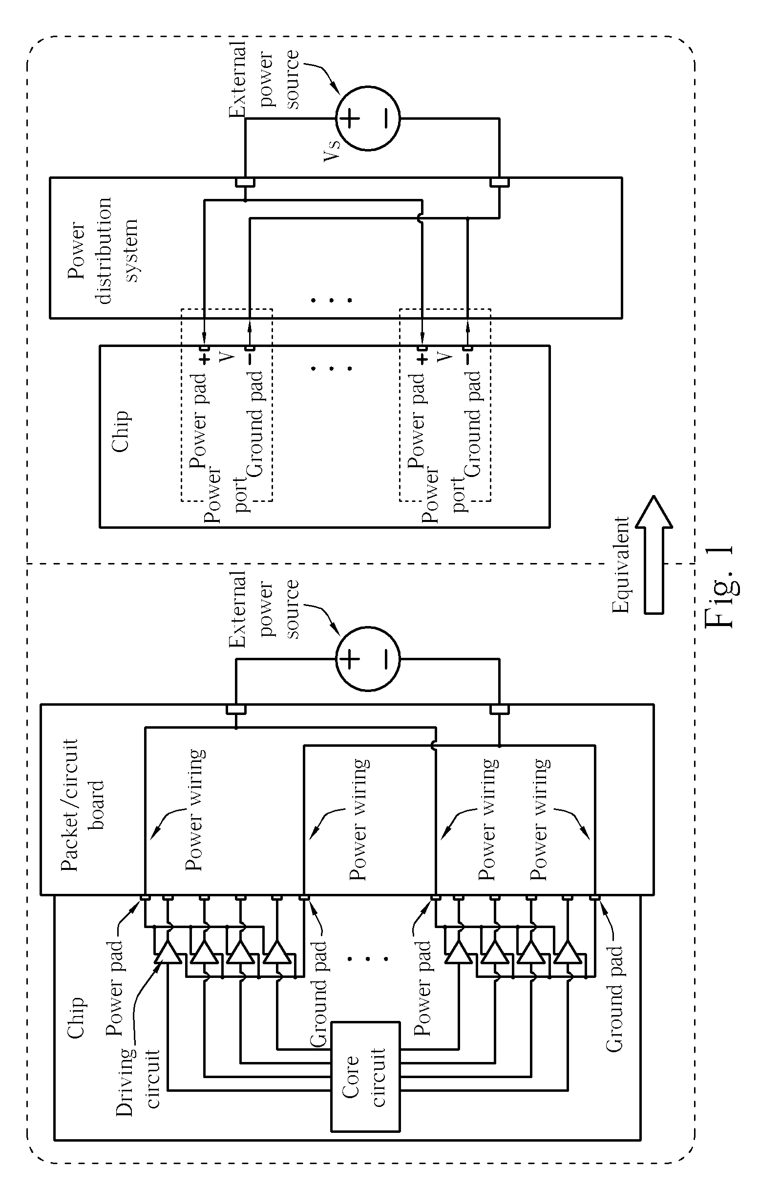
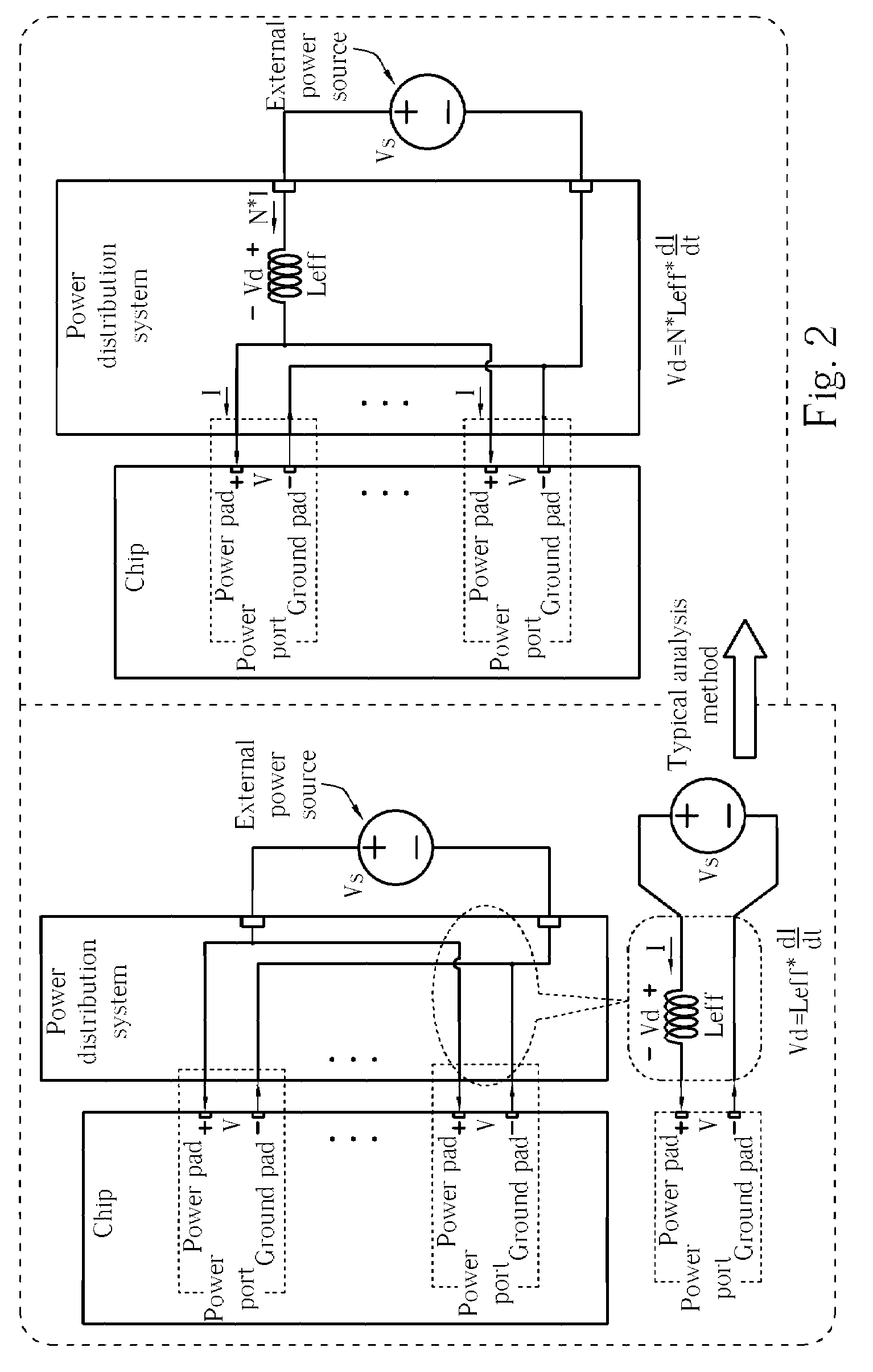
[0022]Please refer to FIG. 1, which is a diagram of a power distribution system and a packaged circuit board corresponding to a chip. As shown in the left side of FIG. 1, the chip is disposed above the packaged circuit board, and the chip has a plurality of power pads and a plurality of ground pads. The plurality of power pads and the plurality of ground pads are connected to the power wiring of the packaged circuit board for transmitting the external supplied power, such as the power provided from a regulator or a power port on a circuit board, to the chip for supplying a required bias current and a required bias voltage.

[0023]In actual applications, pads of a chip may be connected to traces on a packaged circuit board through bonding wires, and the traces are connected to packaged conductive pins so that the pads are connected to an external power through the pins. The combination of the bonding wires, the traces, and the pins is regarded as the power wiring shown in FIG. 1. Moreo...


PUM


Abstract

The methodology includes a single excitation analysis, a multi-excitation analysis, and a simultaneous switch noise, SSN, analysis. A chip connects to the PDS at a plurality of power ports formed by pads for obtaining biasing voltage and current from those power ports. The single excitation analysis includes respectively making each of power ports start conducting current, and measuring a voltage provided by the power port. An equivalent impedance of each power port is obtained. The multi-excitation analysis includes making a given power port conduct a given current, and measuring voltages at other power ports for evaluating mutual couplings across different power ports. The SSN analysis includes respectively making different numbers of power ports conduct currents and accordingly evaluating different equivalent impedances corresponding to different SSN situations.

Description

BACKGROUND OF THE INVENTION[0001]1. Field of the Invention[0002]The present invention relates to an analyzing method and related techniques of a power distribution system, and more particularly, to an analyzing method and related techniques of effectively analyzing couplings between power ports.[0003]2. Description of the Prior Art[0004]In modern society, data and videos may be transmitted, processed, and stored through electronic signals. Therefore, various electronic circuits for processing electronic signals are hardware bases of modern information society.[0005]As known by those skilled in the art, modern electronic circuits are formed on semiconductor chips through semiconductor fabrication processes. However, mechanical properties of the semiconductor chips are fragile, and therefore, the semiconductor chips have to be appropriately packed or be adhered to appropriate encapsulated circuit boards to protect the semiconductor chips. The packaged circuit boards have signal wiring...

Claims


Application Information

Patent Timeline
Patent Type & Authority Patents(United States)
IPC IPC(8): G01R15/00
CPCG06F17/5036G06F2217/78Y04S40/22Y02E60/76G06F30/367G06F2119/06
Inventor HSU, JIMMYHSIAO, RANDY
Owner VIA TECH INC
Why Eureka
Try Eureka