
Versatile system for high-power switching controller in low-power semiconductor technology

Active Publication Date: 2007-09-25
NAT SEMICON CORP
View PDF2 Cites 47 Cited by
  • Summary
  • Abstract
  • Description
  • Claims
  • Application Information

AI Technical Summary

Benefits of technology

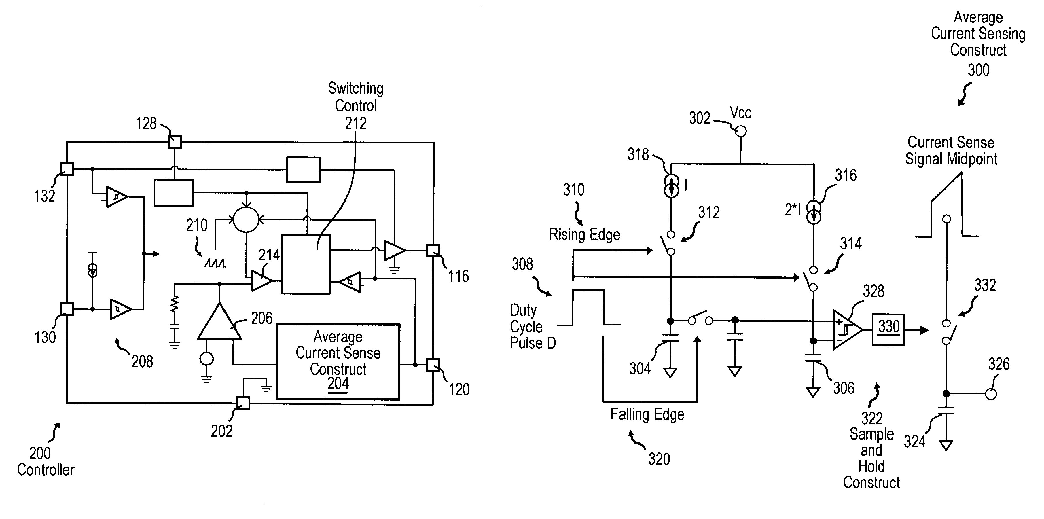
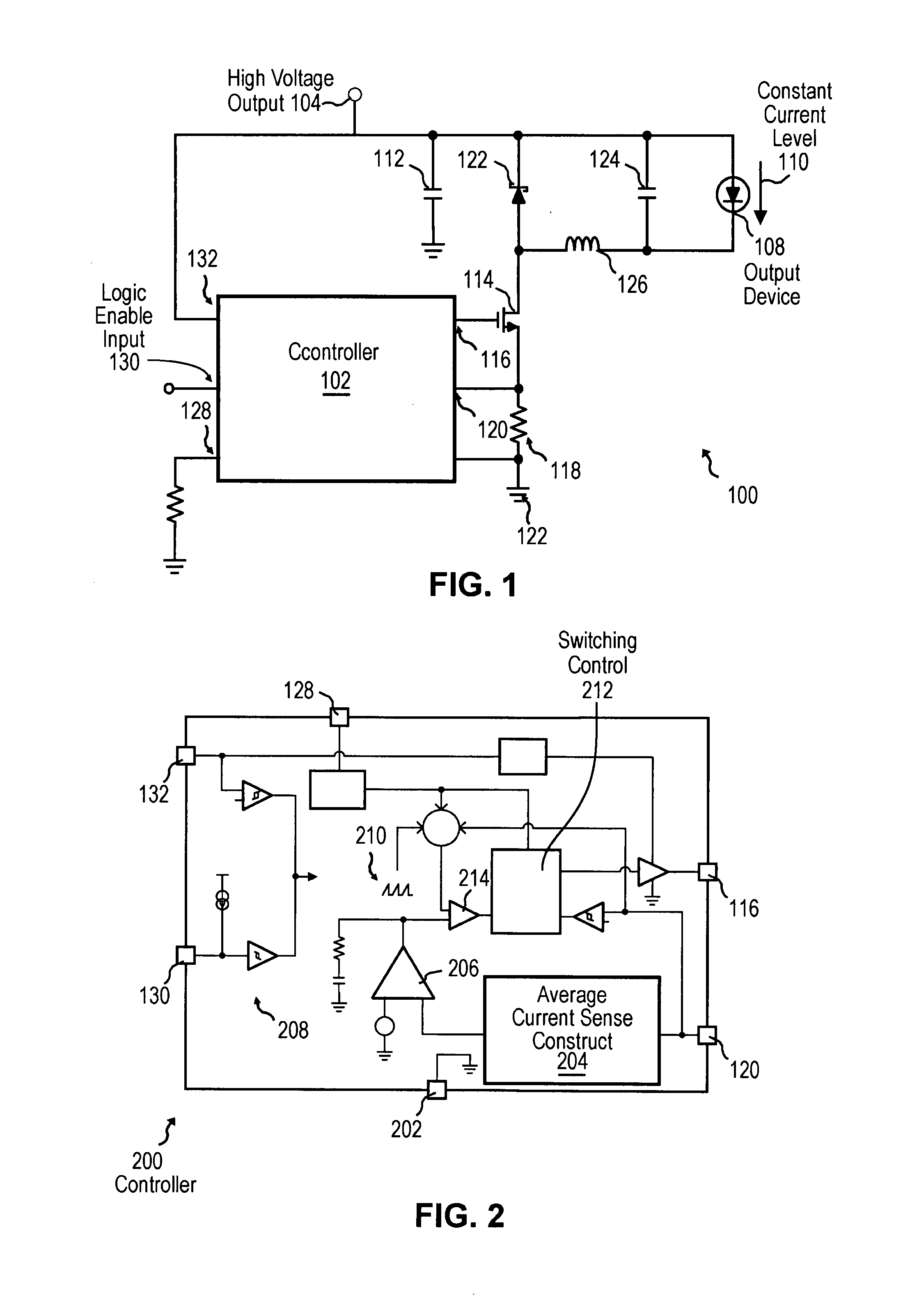
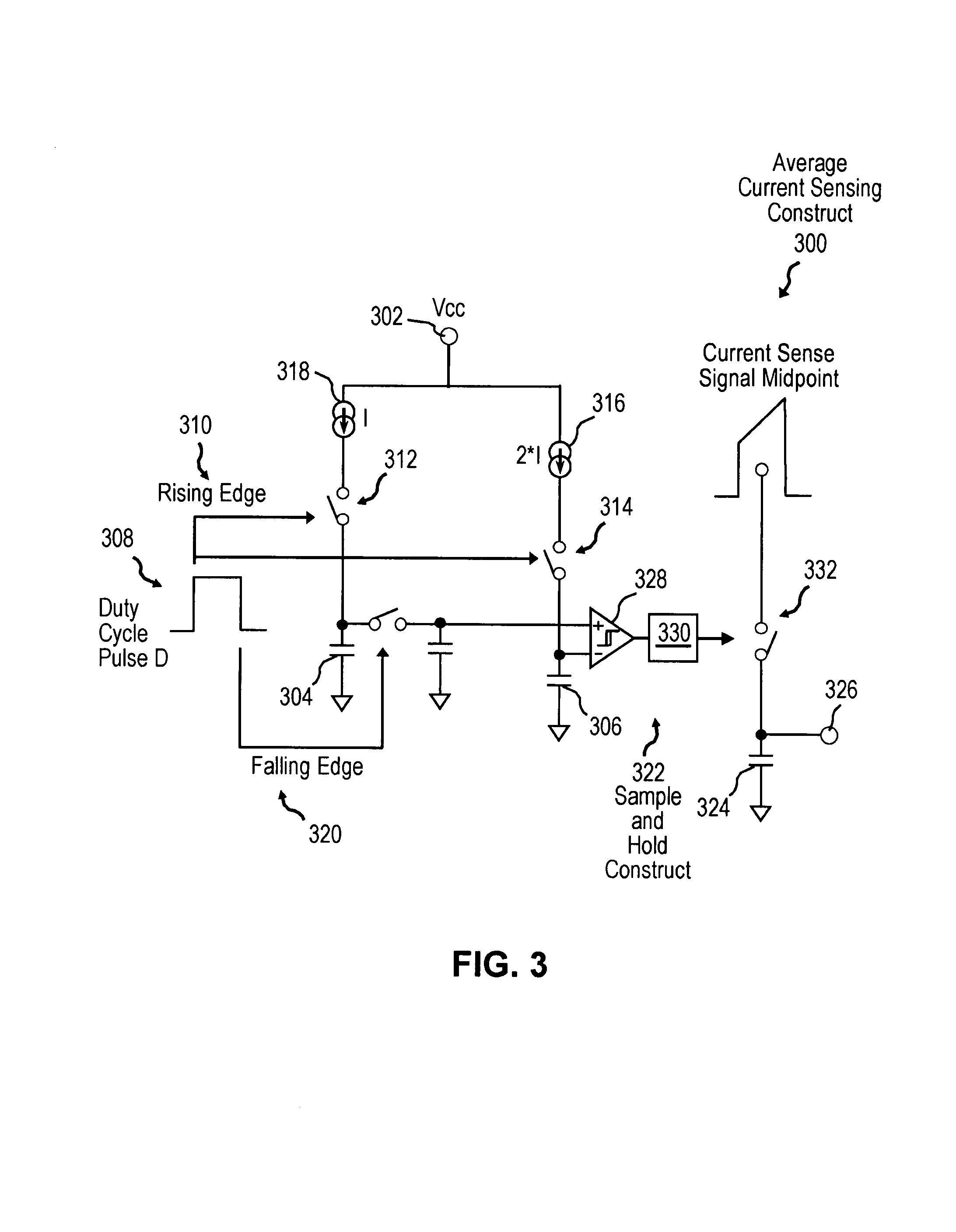
[0013]More specifically, various embodiments of the present invention provide a versatile system for producing a current-mode switching controller—in low voltage commercial semiconductor technologies—that is compatible with applications having very high input voltage ranges. The system provides an output transistor and a sense element coupled to the output transistor. A waveform representative of current charging across the sense element is recognized. First and second charging elements are provided, and the second charging element is adap

Problems solved by technology

In many cases, various electrical components and devices within such products have operational parameters that are not directly compatible with power from a battery supply.
In a number of instances, therefore, devices designed for use in such high voltage applications can not be produced in the most cost-efficient production technologies.
For semiconductor devices, more robust and much more expensive high-voltage process technologies may need to be utilized.
Additionally, or alternatively, lower voltage components may be supplemented with costly discrete components to compensate for voltage differentials.
In either case, these measures result in a more costly or complicated design.
Conventional switching regulators commonly do not address such a need or requirement.
In some cases, such supplementation may be unsuccessful, or marginally effective.
Even where such supplementation may be successful, the additional components can represent a substantial cost increase to the system.

Method used


Image

  • Versatile system for high-power switching controller in low-power semiconductor technology
  • Versatile system for high-power switching controller in low-power semiconductor technology
  • Versatile system for high-power switching controller in low-power semiconductor technology

Examples


Embodiment Construction

[0019]While the making and using of various embodiments of the present invention are discussed in detail below, it should be appreciated that the present invention provides many applicable inventive concepts, which can be embodied in a wide variety of specific contexts. The present invention is hereafter illustratively described in conjunction with the design and operation of switching regulators, optimized for production in low power commercial semiconductor process technologies. Certain aspects of the present invention are further detailed in relation to the design and operation of a low side step-down switching controller device. Although described in relation to such constructs and schemes, the teachings and embodiments of the present invention may be beneficially implemented with a variety of semiconductor devices and technologies. The specific embodiments discussed herein are, therefore, merely demonstrative of specific ways to make and use the invention and do not limit the s...


PUM


Abstract

The present invention provides a versatile system for providing a current-mode switching controller—in low voltage commercial semiconductor technologies—that is compatible with applications having very high input voltage ranges. The system provides an output transistor and a sense element coupled to the output transistor. A waveform representative of current charging across the sense element is recognized. First and second charging elements are provided, and the second charging element is adapted to charge at a rate twice as fast as the first charging element. First and second switching elements, coupled to the first and second charging elements, respectively, are adapted to activate the first and second charging elements responsive to a rising edge of the waveform. An output charge element is provided, and a sample and hold construct is adapted to transfer a charge value—to the output charge element—that corresponds to an average of the charge values of the first and second charging elements upon a falling edge of the waveform.

Description

TECHNICAL FIELD OF THE INVENTION[0001]The present invention relates generally to power regulation components and, more particularly, to a system for providing a high input voltage, current mode switching controller in a low power semiconductor process technology.BACKGROUND OF THE INVENTION[0002]A number of modern electrical systems utilize components having disparate structural or operational characteristics—such as differing power supplies or operational voltage levels. Many consumer products rely on battery power or some combination of battery and continuous power supplies. In many cases, various electrical components and devices within such products have operational parameters that are not directly compatible with power from a battery supply. Frequently, therefore, systems that utilize some form of battery power require conversion of the battery output to levels compatible with the operational characteristics of a system's constituent components.[0003]Consider, for example, autom...

Claims


Application Information

Patent Timeline
IPC IPC(8): G05F1/40
CPCH02M3/156H05B33/0818H05B45/375
Inventor GU, WEIRICHARDSON, CHRISTOPHER B.
Owner NAT SEMICON CORP
Learn More