Semiconductor method and device with mixed orientation substrate

a technology of semiconductor substrate and substrate, applied in the direction of semiconductor/solid-state device details, semiconductor devices, electrical apparatus, etc., can solve the problems of inability to achieve desirable characteristics of p-channel fet formed on the semiconductor substrate having the (100) plane, and the source-drain current of a p-channel fet is inevitably small, so as to reduce the total process steps and relax the critical dimension of the mask

Inactive Publication Date: 2007-11-20
INFINEON TECH AG +1
View PDF28 Cites 453 Cited by
  • Summary
  • Abstract
  • Description
  • Claims
  • Application Information

AI Technical Summary

Benefits of technology

[0012]A further advantage of a preferred embodiment of the present invention is that only two masks are needed and the STI trench definition masks are avoided. Since the active areas are typically larger than the STI, the critical dimension of this mask is relaxed. Further, the total process steps are reduced significantly from a conventional process. Any reduction in process steps and complexity will lead to cost reductions.

Problems solved by technology

However, the mobility of holes is not optimized in the (100) plane, and therefore, the source-drain current of a p-channel FET formed on the semiconductor substrate having the (100) plane is inevitably small.
The p-channel FET therefore fails to have desirable characteristics, even though the n-channel FET exhibits good characteristics.

Method used


Image

  • Semiconductor method and device with mixed orientation substrate
  • Semiconductor method and device with mixed orientation substrate
  • Semiconductor method and device with mixed orientation substrate

Examples


Embodiment Construction

[0017]The making and using of the presently preferred embodiments are discussed in detail below. It should be appreciated, however, that the present invention provides many applicable inventive concepts that can be embodied in a wide variety of specific contexts. The specific embodiments discussed are merely illustrative of specific ways to make and use the invention, and do not limit the scope of the invention.

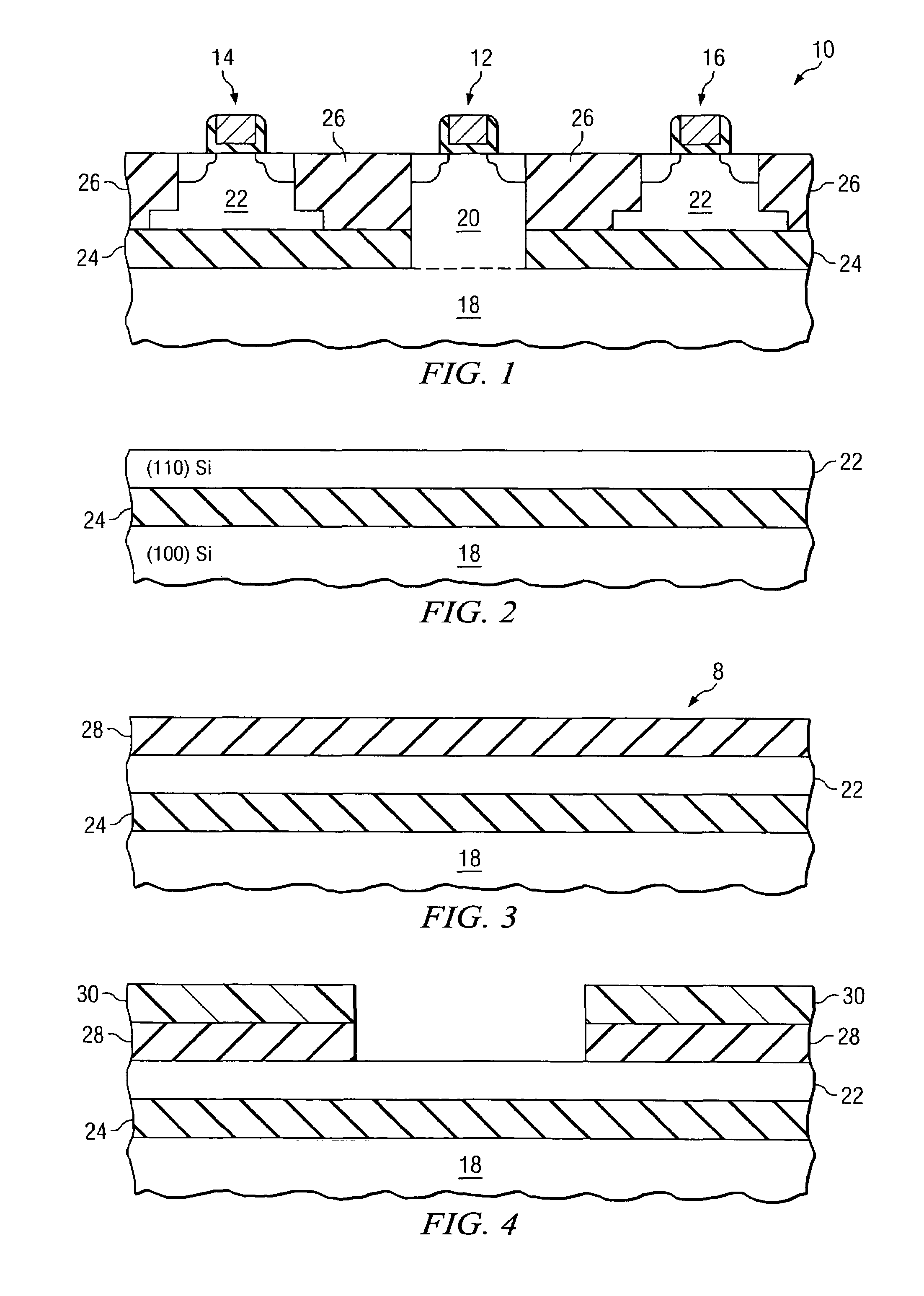
[0018]The present invention will be described with respect to preferred embodiments in a specific context, namely a mixed crystal orientation silicon substrate used to optimize CMOS device performance. The invention may also be applied, however, to other semiconductor devices such as bipolar and BiCMOS and other semiconductors such as silicon germanium.

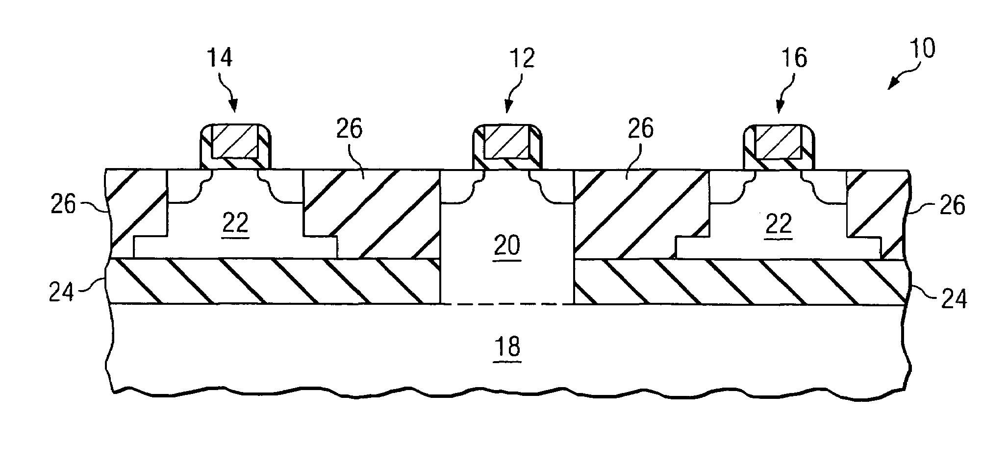
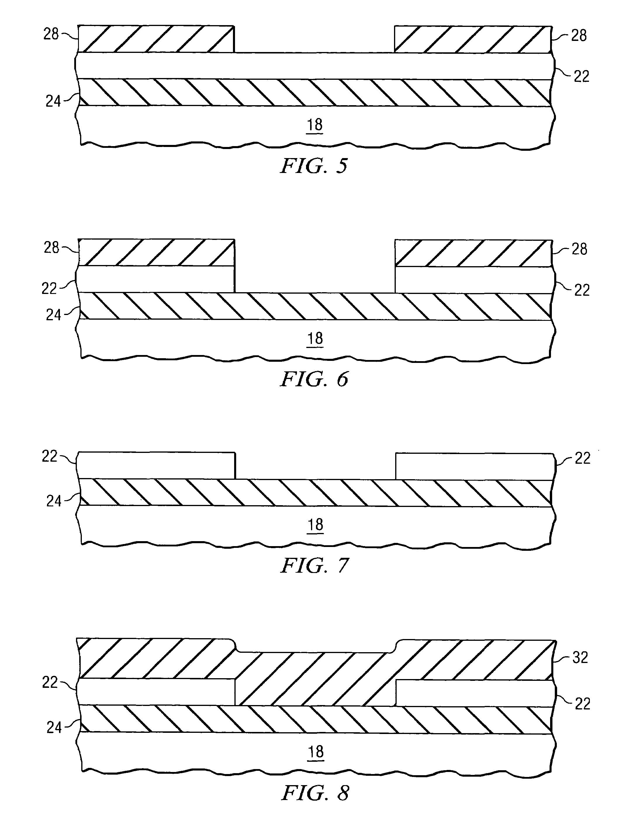
[0019]An exemplary structure of the present invention will be described with respect to FIG. 1. A process flow for manufacturing this structure will then be described with reference to FIGS. 2-16. An alternative structure is sh...


PUM


Abstract

A semiconductor device includes a semiconductor body having semiconductor material of a first crystal orientation. A first transistor is formed in the semiconductor material of the first crystal orientation. An insulating layer overlies portions of the semiconductor body and a semiconductor layer overlies the insulating layer. The semiconductor layer has a second crystal orientation. A second transistor is formed in the semiconductor layer having the second crystal orientation. In the preferred embodiment, the semiconductor body is (100) silicon, the first transistor is an NMOS transistor, the semiconductor layer is (110) silicon and the second transistor is a PMOS transistor.

Description

TECHNICAL FIELD[0001]The present invention relates generally to semiconductor devices, and more particularly to a semiconductor method and device with mixed orientation substrate.BACKGROUND[0002]Complementary metal oxide semiconductor (CMOS) is a dominant technology in semiconductor device manufacture. A CMOS device includes both n-channel (NMOS) and p-channel (PMOS) transistors. In CMOS technology, both kinds of transistors are used in a complementary way to form a current gate that forms an effective means of electrical control. Advantageously, CMOS transistors use very little power when not switching from one state to another.[0003]It is known that the mobility of carriers is dependent on a number of factors, especially the surface plane of a wafer. Conventional silicon substrates typically have a surface oriented on the (100) crystal plane. In this plane, the mobility of electrons is higher than in other crystal planes, and therefore, the source-drain current of an n-channel FET...

Claims


Application Information

Patent Timeline
Patent Type & Authority Patents(United States)
IPC IPC(8): H01L27/12
CPCH01L21/76232H01L21/76283H01L21/823807H01L21/823878H01L27/1207H01L27/1203H01L29/045H01L21/84H01L29/78687
Inventor YAN, JIANGSUNG, CHUN-YUNGSHUM, DANNY PAK-CHUMGUTMANN, ALOIS
Owner INFINEON TECH AG
Why Eureka
Try Eureka