Dual silicide process to improve device performance

a technology of suicide contact and mosfet, which is applied in the direction of semiconductor devices, electrical equipment, transistors, etc., can solve the problems of reducing and mosfets beginning to reach their traditional scaling limits, so as to reduce the resistance of mosfets

Inactive Publication Date: 2006-07-27
IBM CORP
View PDF13 Cites 68 Cited by
  • Summary
  • Abstract
  • Description
  • Claims
  • Application Information

AI Technical Summary

Benefits of technology

[0013] An object of the present invention is to provide a semiconducting contact structure havin

Problems solved by technology

Additionally, prior contacts have utilized very high dopant concentrations to reduce contact resistance.
However, there are growing signs today that MOSFETs are beginning to reach their traditional scaling limits.
Since it has b

Method used


Image

  • Dual silicide process to improve device performance
  • Dual silicide process to improve device performance
  • Dual silicide process to improve device performance

Examples


first embodiment

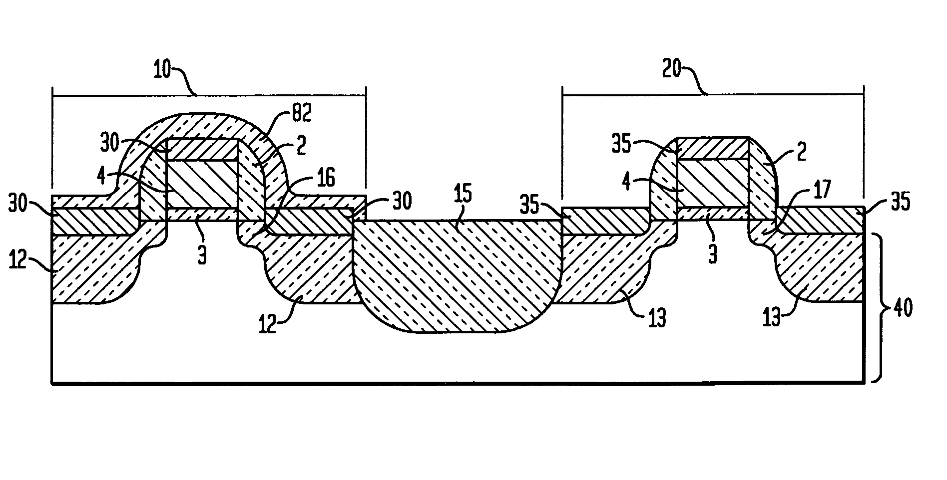
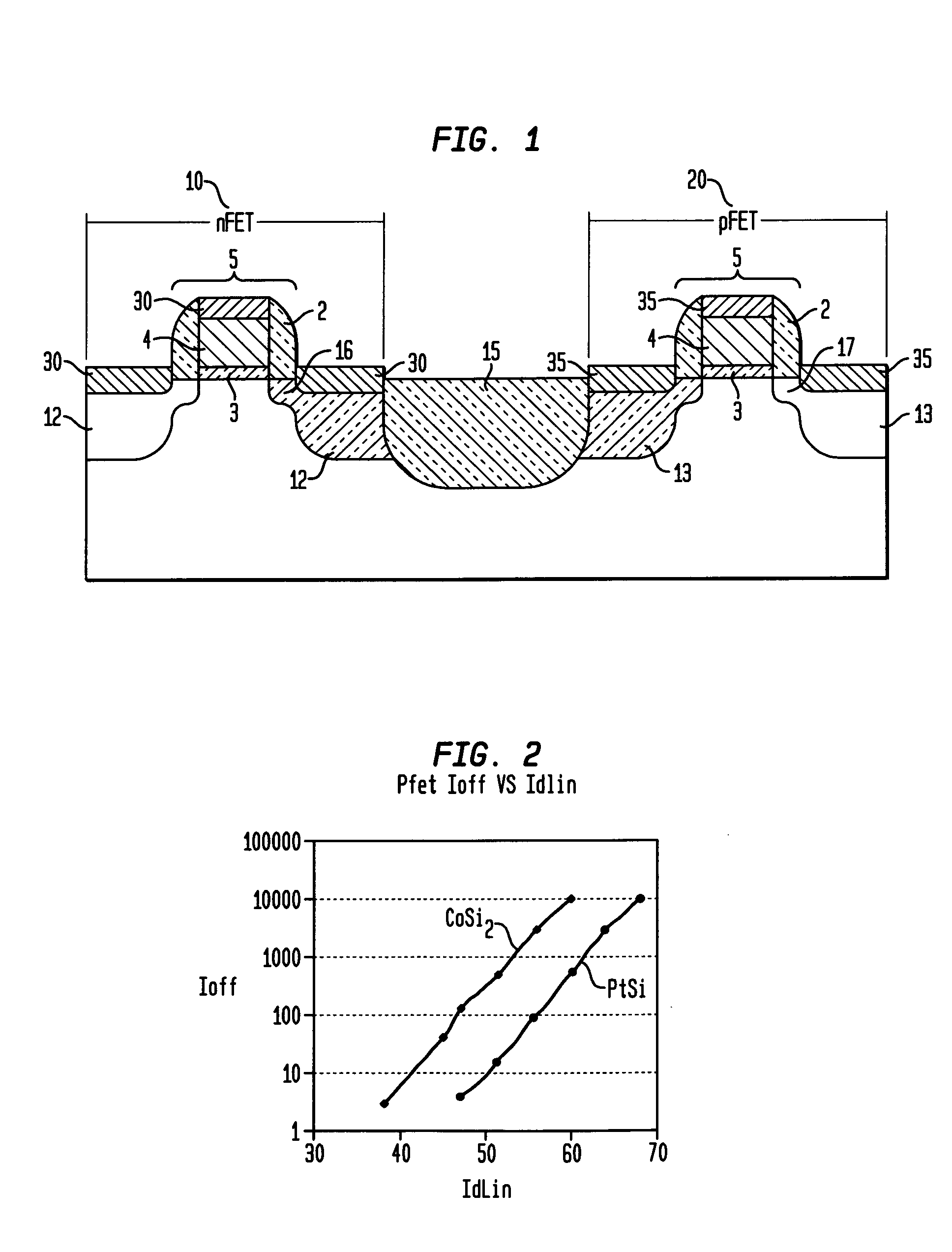
[0060] The method for forming the above-described semiconducting structure, as depicted in FIG. 1, is now described with reference to FIGS. 3-10. the inventive method is depicted in FIGS. 3-5 which depict (through cross sectional view) one embodiment of the inventive method for providing a CMOS structure having low resistance metal suicide contacts to pFET device and a different low resistance metal suicide contacts to nFET device regions with the suicide differences tailored to improve contact resistances for the differing device types.

[0061] Referring to FIG. 3, an initial structure is provided having nFET device regions 10 and PFET device regions 20 formed on a substrate 40 of silicon (Si)-containing material. Si-containing materials include, but are not limited to: silicon, single crystal silicon, polycrystalline silicon, silicon germanium, silicon-on-silicon germanium, amorphous silicon, silicon-on-insulator (SOI), silicon germanium-on-insulator (SGOI), and annealed polysilicon...

second embodiment

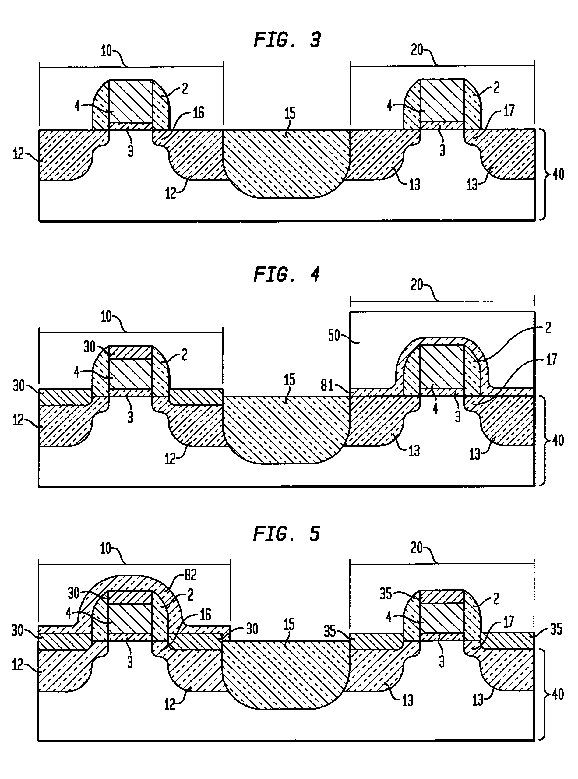
[0087] Referring now to FIG. 6, in the present invention, following the formation of the low resistance n-type silicide contact 30, the first protective layer is removed from the substrate 40 and a second metal layer 45 is deposited directly atop the low resistance n-type silicide contact 30 in the nFET device region 10 and the substrate 40 surface of the pFET device region 20. The first protective layer is removed by a highly selective etch process that removes the first block mask without substantially etching the formed n-type silicide contact 30 or the surface of the p-type device region 20.

[0088] Following first protective layer removal, the surface of the low resistance n-type silicide contact 30 and the p-type device region 20 are then cleaned to provide a clean surface for silicidation. The cleaning process may be a conventional chemical clean as known within the skill of the art.

[0089] A second metal layer 45 is then deposited directly atop the pFET device region 20 and th...


PUM


Abstract

A semiconducting structure and a method of forming thereof, includes a substrate having a p-type device region and an n-type device region; a first-type suicide contact to the n-type device region; the first-type suicide having a work function that is substantially aligned to the n-type device region conduction band; and a second-type silicide contact to the p-type device region; the second-type silicide having a work function that is substantially aligned to the p-type device region valence band. The present invention also provides a semiconducting structure and a method of forming therefore, in which the silicide contact material and silicide contact processing conditions are selected to provide strain based device improvements in pFET and nFET devices.

Description

FIELD OF THE INVENTION [0001] The present invention relates to metal suicide contacts for use in semiconductor devices, and more particularly to a structure, and a method of forming thereof, having two different metal silicide contacts with two different work functions. The present invention also relates to semiconductor devices, in which the metal of the silicide contact is selected to provide strain based device improvements. BACKGROUND OF THE INVENTION [0002] In order to be able to fabricate integrated circuits (ICs) of increased performance than is currently feasible, device contacts must be developed which reduce the electrical contact resistance. A contact is the electrical connection between an active semiconductor device region, e.g., a source / drain or gate of a transistor device at the wafer surface, and a metal layer, which serve as interconnects. [0003] Silicide contacts are of specific importance to IC's, including complementary metal oxide semiconductor (CMOS) devices b...

Claims


Application Information

Patent Timeline
IPC IPC(8): H01L29/76
CPCH01L21/28052H01L21/823814H01L21/823835H01L29/4933H01L29/665H01L29/6659H01L29/7833H01L29/7845
Inventor ELLIS-MONAGHAN, JOHN J.MARTIN, DALE W.MURPHY, WILLIAM J.NAKOS, JAMES S.PETERSON, KIRK D.
Owner IBM CORP
Why Eureka
Try Eureka