Method for forming microelectronic spring structures on a substrate

a micro-electronic spring and substrate technology, applied in the field of lithographic scale, micro-electronic spring contacts, can solve the problems of unsuitable prior art manufacturing methods for making lithographic type spring contacts, the cost of fabricating fine-pitch spring contacts has limited the range of applicability to less cost-sensitive applications, and the cost of manufacturing equipment and process tim

Inactive Publication Date: 2001-11-22
FORMFACTOR INC
View PDF49 Cites 73 Cited by
  • Summary
  • Abstract
  • Description
  • Claims
  • Application Information

AI Technical Summary

Problems solved by technology

In practice, however, the cost of fabricating fine-pitch spring contacts has limited their range of applicability to less cost-sensitive applications.
Much of the fabrication cost is associated with manufacturing equipment and process time.
However, prior art manufacturing methods are unsuitable for making lithographic type spring contacts with such suitably contoured, non-rectangular cross-sections, and other types of more complex shapes.
However, the use of multiple layers adds undesirable cost and complexity to the manufacturing process.
Layered structures are also subject to undesirable stress concentration and stress corrosion cracking, because of the discontinuities (i.e., stepped structures) that result from layering processes.
Similar difficulties may be encountered when sputtering over a layer of sacrificial material, which typically is an organic material that may also contain

Method used


Image

  • Method for forming microelectronic spring structures on a substrate
  • Method for forming microelectronic spring structures on a substrate
  • Method for forming microelectronic spring structures on a substrate

Examples


Embodiment Construction

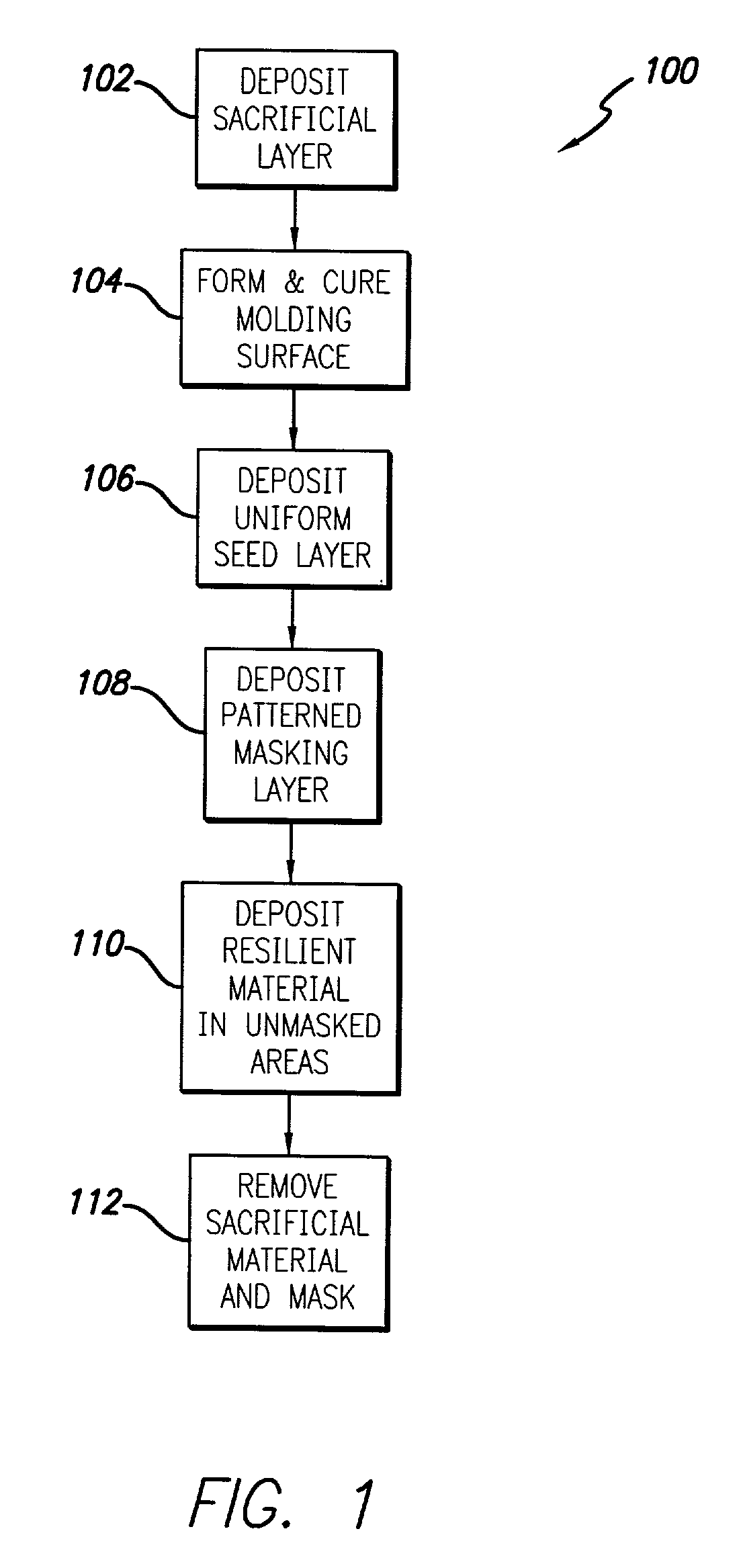
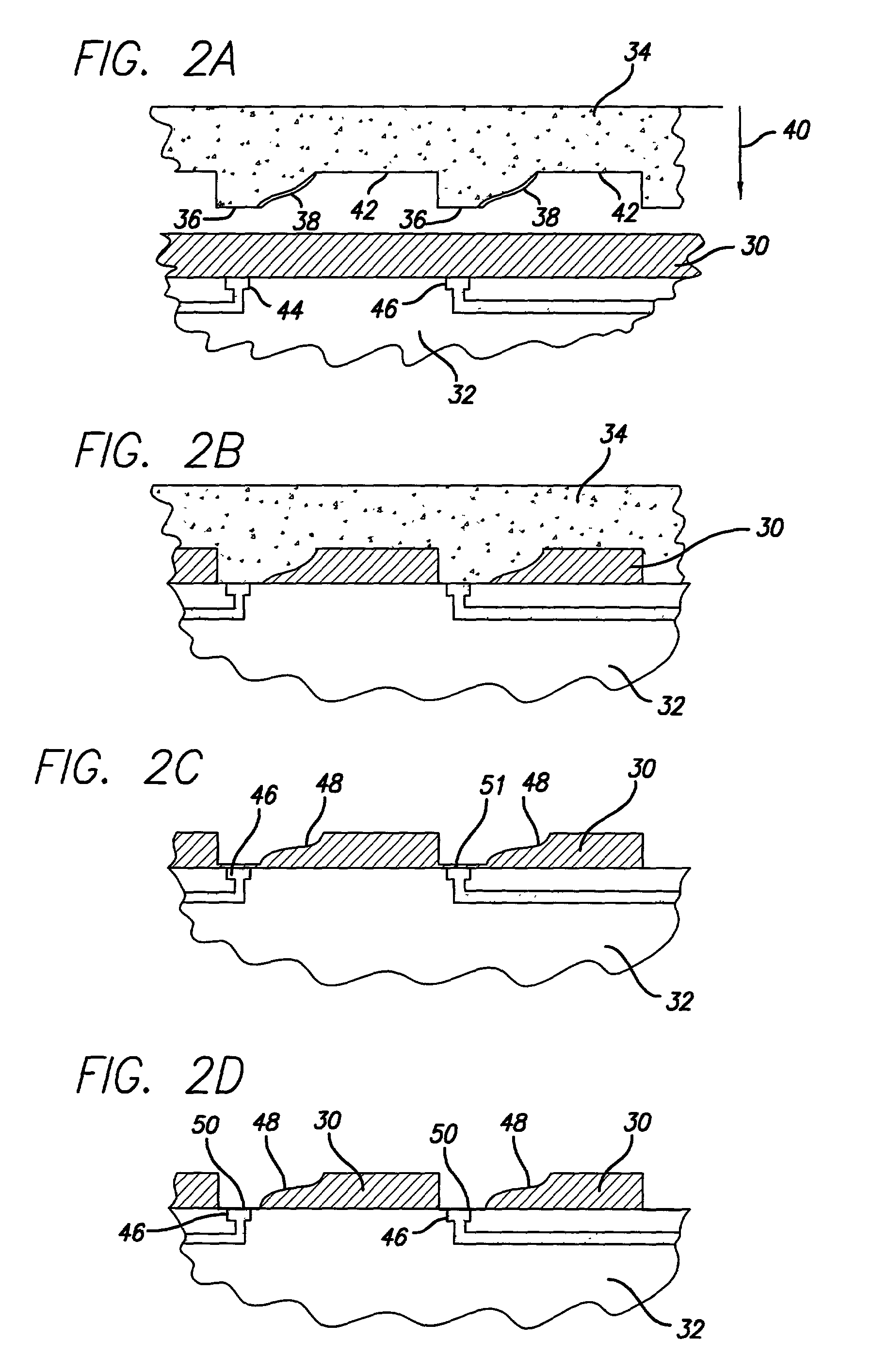
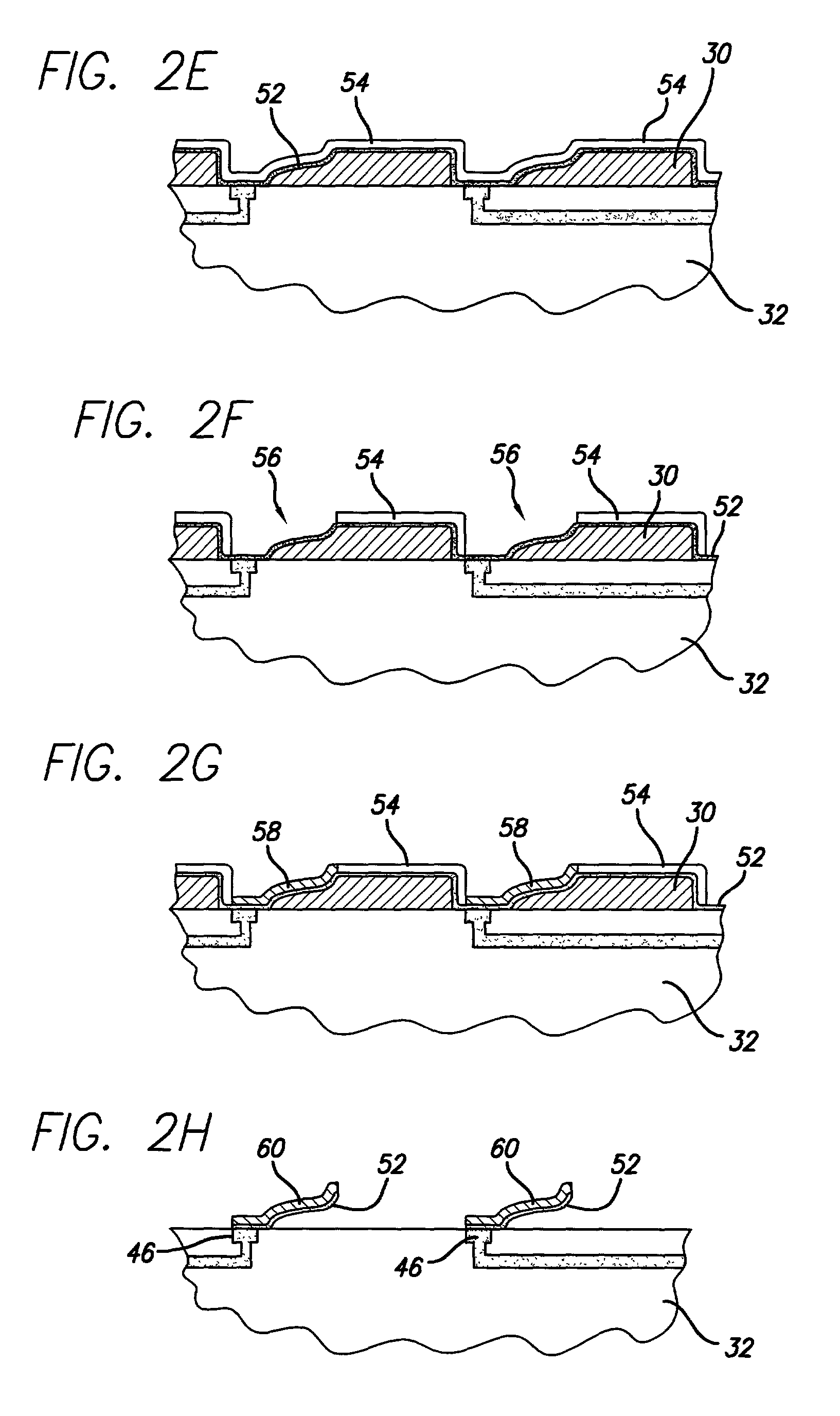
[0114] A silicon wafer with a 0.5 micron surface oxide layer was selected for a prototype substrate. A layer of chrome was sputtered on a surface of the substrate, followed by a layer of gold, to provide a shorting layer. A 4.0 mil (100 micron) thick layer of negative dry-film photoresist was applied to the sputtered gold layer using a vacuum laminator. A second 3.0 mil (75 micron) thick layer of the same type of photoresist was applied over the first layer. The substrate was placed on a hot plate and heated until the photoresist was soft. An embossing tool with protruding triangular teeth contoured to produce the desired spring shape was pressed into the photoresist laminate while the laminate was soft. The substrate was cooled and the embossing tool was removed. A photolithography mask and UV light were used to expose (and thus cross link) the photoresist laminate everywhere except in the area of the spring base contact. The photoresist was developed using a spray developer with s...


PUM

PropertyMeasurementUnit
Pressureaaaaaaaaaa
Angleaaaaaaaaaa
Areaaaaaaaaaaa

Abstract

A method for fabricating microelectronic spring structures is disclosed. In an initial step of the method, a layer of sacrificial material is formed over a substrate. Then, a contoured surface is developed in the sacrificial material, such as by molding the sacrificial material using a mold or stamp. The contoured surface provides a mold for at least one spring form, and preferably for an array of spring forms. If necessary, the sacrificial layer is then cured or hardened. A layer of spring material is deposited over the contoured surface of the sacrificial material, in a pattern to define at least one spring form, and preferably an array of spring forms. The sacrificial material is then at least partially removed from beneath the spring form to reveal at least one freestanding spring structure. A separate conducting tip is optionally attached to each resulting spring structure, and each structure is optionally plated or covered with an additional layer or layers of material, as desired. An alternative method for making a resilient contact structure using the properties of a fluid meniscus is additionally disclosed. In an initial step of the alternative method, a layer of material is provided over a substrate. Then, a recess is developed in the material, and fluid is provided in the recess to form a meniscus. The fluid is cured or hardened to stabilize the contoured shape of the meniscus. The stabilized meniscus is then used to define a spring form in the same manner as the molded surface in the sacrificial material.

Description

[0001] This application is a continuation-in-part of the co-pending U.S. patent application Ser. No. 09 / 710,539, filed Nov. 9, 2000, entitled "LITHOGRAPHIC SCALE MICROELECTRONIC SPRING STRUCTURES WITH IMPROVED CONTOURS," by Eldridge and Wenzel (hereinafter the "FIRST PARENT CASE"), which is a continuation-in-part of co-pending application Ser. No. 09 / 364,788, filed Jul. 30, 1999, entitled "INTERCONNECT ASSEMBLIES AND METHODS," by Eldridge and Mathieu (hereinafter, the "SECOND PARENT CASE"), which applications are incorporated herein, in their entirety, by reference.[0002] 1. Field of the Invention[0003] The present invention relates to electrical contact elements for electrical devices, and more particularly to lithographic-scale, microelectronic spring contacts with improved contours.[0004] 2. Description of Related Art[0005] Recent technological advances, such as described in U.S. Pat. No. 5,917,707 to Khandros et al., have provided small, flexible and resilient microelectronic sp...

Claims


Application Information

Patent Timeline
IPC IPC(8): B81C1/00B81B3/00G01R1/04G01R1/067G01R1/073G01R3/00H01H11/04H01L21/768H01L23/48H01L23/482H01R13/24H05K3/40H05K7/10
CPCG01R1/0483Y10T29/49147G01R1/06733G01R1/07342G01R3/00H01L23/4822H01L24/72H01L2924/01002H01L2924/01004H01L2924/01011H01L2924/01013H01L2924/01015H01L2924/01027H01L2924/01029H01L2924/01033H01L2924/01042H01L2924/01046H01L2924/01049H01L2924/01074H01L2924/01075H01L2924/01078H01L2924/01079H01L2924/01082H01L2924/14H01L2924/3025H01R13/24H01R13/2407H05K3/4092H05K7/1069H01R12/52H01L2924/01005H01L2924/01006H01L2924/01023H01L2924/01024H01L2924/01047H01L2924/10253G01R1/06716G01R1/06727H01L2924/00H01L2924/12036H01L2924/12042H01L2924/181H01L23/48
Inventor ELDRIDGE, BENJAMIN N.WENZEL, STUART W.
Owner FORMFACTOR INC
Why Eureka
Try Eureka