Method of making interband tunneling diodes

a tunneling diode and interband technology, applied in the direction of diodes, semiconductor devices, electrical apparatus, etc., can solve the problems of undesirable broadening of the -doping plane, kinetic growth of the -doping layer, and the inability to build n-type rtd in si

Inactive Publication Date: 2007-12-04
THE OHIO STATES UNIV +1
View PDF1 Cites 10 Cited by
  • Summary
  • Abstract
  • Description
  • Claims
  • Application Information

AI Technical Summary

Benefits of technology

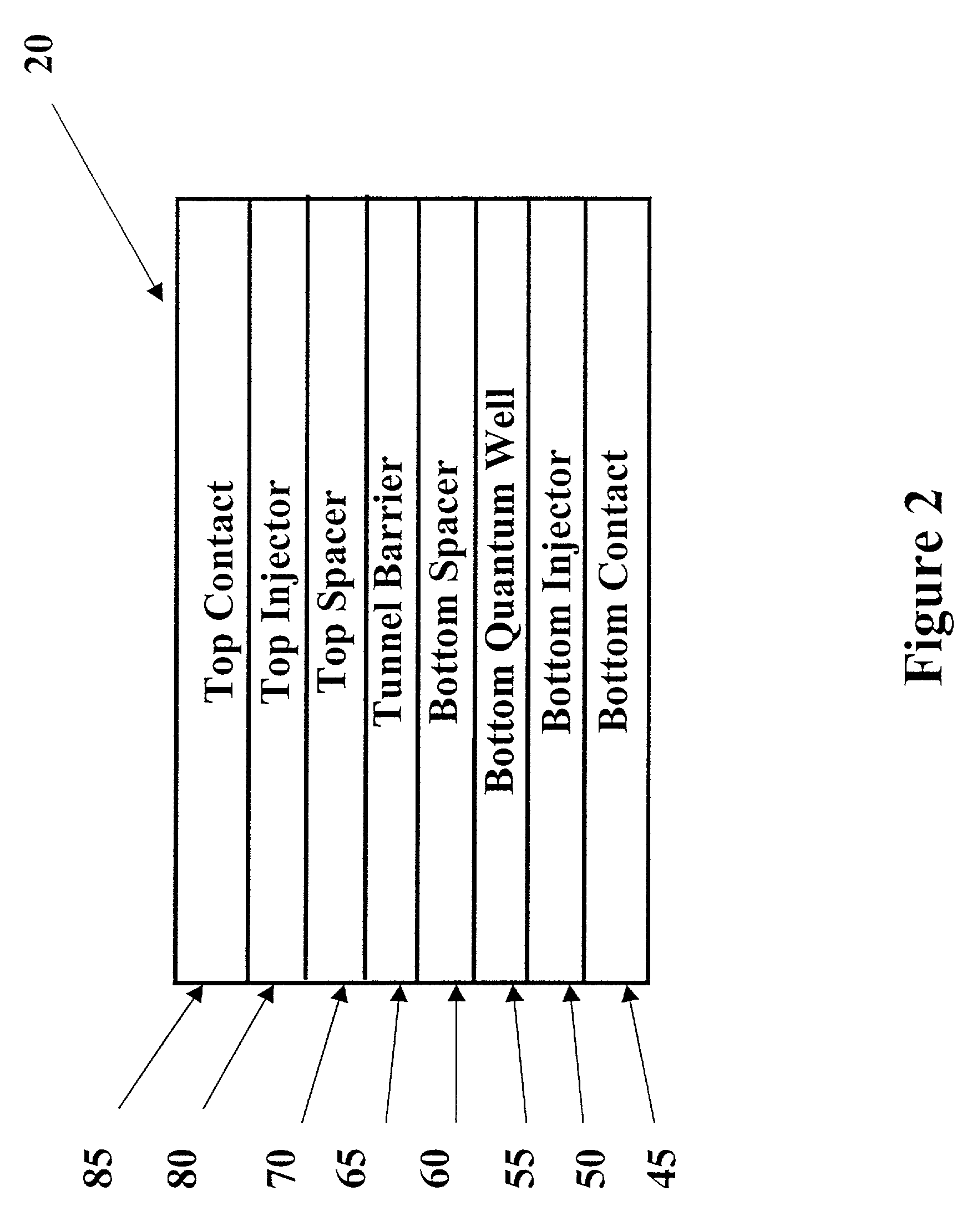
[0041]An additional embodiment of the invention results from the growth of a pnp (or npn) tunnel diode with dual tunnel barriers. One feature of this layer is that its electrical characteristics are symmetrical with applied bias, resulting in the onset of negative differential resistance in the forward and reverse directions. The structure is defined by a P+ (or N+) ohmic contact layer, a P+(or N+) injection layer, a quantum well (the quantum well may be defined by delta doping, band discontinuities resulting from heterojunction interfaces, superlattices, or a combination thereof) in the valence (or conduction) band with, a tunnel barrier (doped or undoped) sandwiched between a pair of spacer layers (doped or undoped), a quantum well (the quantum well may be defined by delta doping, band discontinuities resulting from heterojunction interfaces, superlattices, or a combination thereof) in the conduction (or valence) band with, a second tunnel barrier (doped or undoped) sandwiched between a pair of spacer layers (doped or undoped), a quantum well (the quantum wee may be defined by delta doping, band discontinuities resulting from heterojunction interfaces, superlattices, or a combination thereof) in the valence (or conduction) band with, a P+ (or N+) injection layer, and a P+ (or N+) contact layer.

Problems solved by technology

However, an n-type RTD is not particularly feasible to build in Si.
In reality, the growth of a δ-doping layer is kinetically limited.
Phenomena such as segregation and diffusion will result in undesirable broadening of the δ-doping planes.
Growth at reduced temperatures, however, will almost certainly produce films of increased defect densities.
This leads to two results: monotonically abrupt doping profiles and an amorphous epitaxial layer.
One problem with SPE is that electrical activity falls below unity, particularly for Sb [23].
Since the undesirable excess current component of tunnel diodes is believed to be defect mediated, highly defected growth is unacceptable for tunnel diode growth.
While low temperature molecular beam epitaxy (LT-MBE) will not allow for profiles as sharply defined as those formed by SPE, it is sufficient to substantially suppress dopant segregation.
Even the excellent results at 320° C., however, still suffer from moderate segregation.
Achieving sharp, arbitrary n-type doping profiles during Si and SiGe MBE is challenging and several approaches have been investigated to overcome the high surface segregation ratio of P, As, and Sb [25].
Each has its limitations and for the latter technique it is one primarily of cost and complexity.
Film quality is however compromised in return for achieving active Sb doping levels in excess of 5×1020 cm−3.
The technique indeed produces sharp doping profiles although the high temperature step leads to undesirable dopant diffusion and constrains the maximum carrier concentration to solid solubility limits [28].
Growth at temperatures as low as 220° C. clearly results in strong RHEED oscillations.
Growth at 50° C. shows severely damped oscillations, suggesting that 50° C. will not yield a good film.
Films grown by SPE suffer from incomplete dopant activation.
Of course, it is expected that films grown by LT-MBE will have more defects than those grown by standard MBE temperatures.
It is believed that LT-MBE leads to the presence of vacancy-like defects throughout the film [36].
The entire structure was grown around 500-550° C., which was too high and led to deleterious dopant segregation and diffusion.

Method used


Image

  • Method of making interband tunneling diodes
  • Method of making interband tunneling diodes
  • Method of making interband tunneling diodes

Examples


example 1

[0083]This example illustrates an embodiment of a SiGe Heterojunction Esaki which takes advantage of the natural band offsets between Si and Si0 5Ge0.5 to lower the doping requirements on the P+ side of the junction. This structure is shown in FIG. 4 with an accompanying electrostatic band diagram. A 10 nm digitally graded superlattice (DG-SL) was incorporated on the P+ side of the junction to reduce the barrier for holes to populate the valence band well. Similar structures incorporated as part of InP based MSM photodetectors have been used to enhance the bandwidth, and this was a secondary motivation here [58]. In order to lower the current density for potential low power memory applications, a 4 nm intrinsic Si spacer was placed between the P++ and N++ layers. FIG. 5 demonstrates the I-V characteristics of this structure. NDR was observed for a 600° C., 1 min. anneal. The PVCR was found to be 1.2 at a low current density of 7.5 A / cm2.

example 2

[0084]Schematic diagrams of the RITDs examined in this embodiment are shown in FIG. 6. FIG. 6(a) shows one configuration of the RITD, TD1, which employed a 4 nm undoped Si0.5Ge0.5 tunneling barrier and δ-doping planes at the Si / SiGe heterointerface. FIG. 6(b) shows another configuration, TD2, which was identical to TD1 described above, except that both δ-doping planes were offset from the Si / SiGe heterointerface with 1 nm of undoped Si on either side of the Si0.5Ge0.5 tunneling barrier. Portions of each wafer were annealed in an AG Associates Heat Pulse 610 RTA at 600° C., 700° C., or 800° C. All anneal times were fixed at 1 minute.

[0085]As-grown samples show very weak inflections near the origin when unannealed. The diode performance was improved at 600° C. 1 min annealing conditions, showing a slight inflection in the I-V near 0.4 V. No NDR was evident in this layer either. For both structures, samples were annealed at 700° C. and 800° C., 1 min. The results for these two samples ...

example 3

[0087]In order to address the influence of the offset in δ-doping from the heterointerface, additional layers may be fabricated. These layers, referred to as TD4 and TD5, are shown schematically in FIGS. 10 and 11, respectively. The distance between the δ-doping planes, including both the Si and SiGe layers, was fixed at 4 nm in both layers to allow a direct comparison with TD1 and TD3. The Si0.5Ge0.5 layer in TD3 was 3 nm thick, and in TD4 was 1 nm thick. Based on the previous studies, it was determined that an advantageous anneal for this structure was 700° C., 1 min. Therefore, as a comparison, both of these samples were annealed under this condition, and also at 600° C., 1 min.

[0088]The portions of both sample annealed at 600° C., 1 min only showed weak inflections in the forward directions. Consistent with the other samples investigated, NDR was observed for a 700° C., 1 min anneal. Dramatically different performance was observed between the two samples. The current density obs...


PUM


Abstract

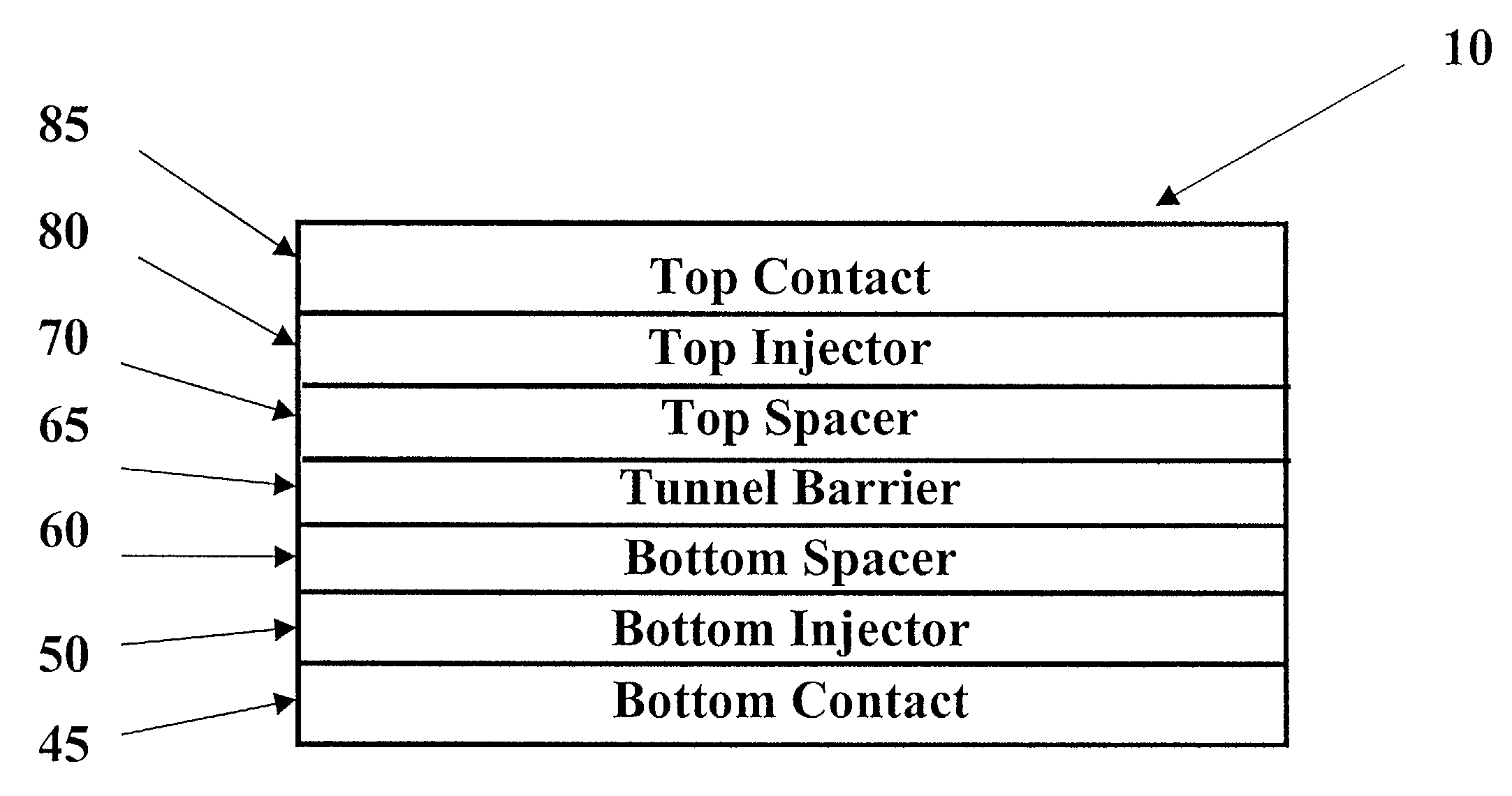
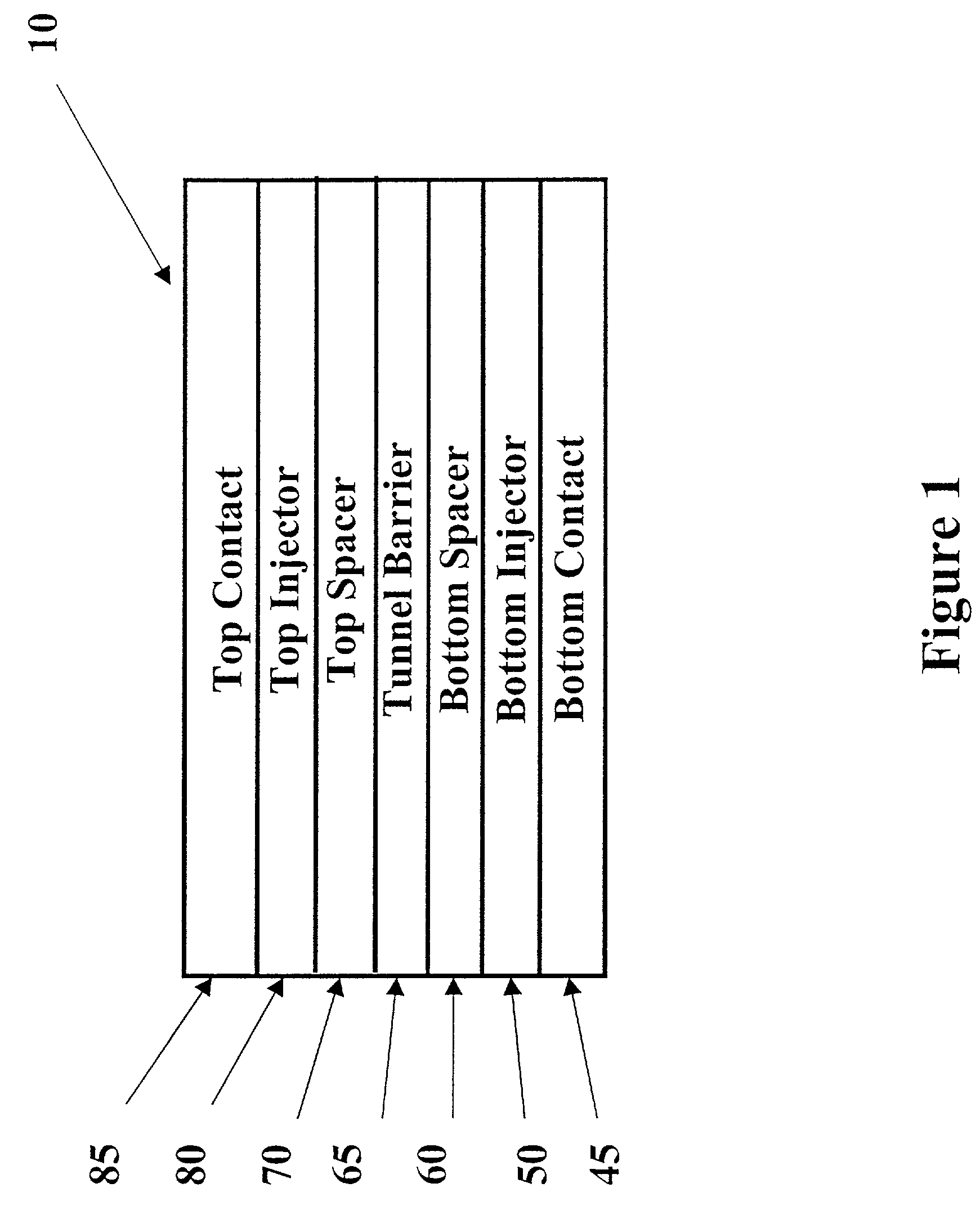
Interband tunnel diodes which are compatible with Si-based processes such as, but not limited to, CMOS and SiGe HBT fabrication. Interband tunnel diodes are disclosed (i) with spacer layers surrounding a tunnel barrier; (ii) with a quantum well adjacent to, but not necessarily in contact with, one of the injectors, and (iii) with a first quantum well adjacent to, but not necessarily in contact with, the bottom injector and a second quantum well adjacent to, but not necessarily in contact with, the top injector. Process parameters include temperature process for growth, deposition or conversion of the tunnel diode and subsequent thermal cycling which to improve device benchmarks such as peak current density and the peak-to-valley current ratio.

Description

[0001]This application is a divisional of application Ser. No. 09 / 565,455, filed on May 5, 2000, now U.S. Pat. No. 6,803,598, the entire contents of which are hereby incorporated by reference and for which priority is claimed under 35 U.S.C. § 120; and this application claims priority of application Ser. No. 60 / 133,067 filed in the U.S. on May 7, 1999 under 35 U.S.C. § 119.[0002]The present application has Government rights assigned to the National Science Foundation under contract numbers ECS-9622134 and ECS-9624160, and assigned to DARPA / AFOSR under contract number F49620-96-C-0006.BACKGROUND OF THE INVENTION[0003]A. Field of the Invention[0004]The present invention relates generally to interband tunneling diodes, and, more particularly to Si-based resonant interband tunneling diodes and a method of making interband tunneling diodes.[0005]B. Description of the Related Art[0006]The purpose of this invention is the development of a tunnel diode exhibiting negative differential resis...

Claims


Application Information

Patent Timeline
Patent Type & Authority Patents(United States)
IPC IPC(8): H01L21/20H01L21/329H01L29/88
CPCB82Y10/00H01L29/66151H01L29/882Y10S438/979Y10S438/983
Inventor BERGER, PAUL R.THOMPSON, PHILLIP E.LAKE, ROGERHOBART, KARLROMMEL, SEAN L.
Owner THE OHIO STATES UNIV
Why Eureka
Try Eureka