Apparatus and method of interconnecting nanoscale programmable logic array clusters

a technology clusters, applied in the field of programmable logic arrays, can solve the problems of nanoplas very long wires, difficult to manufacture long nanowires without defects, and nanoscale diameter wires that tend to break during assembly

Inactive Publication Date: 2007-12-18
CALIFORNIA INST OF TECH
View PDF21 Cites 16 Cited by
  • Summary
  • Abstract
  • Description
  • Claims
  • Application Information

AI Technical Summary

Problems solved by technology

When building large nanoPLAs, the wires in the nanoPLAs will become very long.
Long nanowires are difficult to manufacture without defects and can be very slow.
In particular, the nanoscale diameter wires tend to break during assembly when their length becomes many tens of microns in length.
Further, the resistance of the small diameter nanowires becomes larger with the length of the nanowires making PLA operation slower.

Method used


Image

  • Apparatus and method of interconnecting nanoscale programmable logic array clusters
  • Apparatus and method of interconnecting nanoscale programmable logic array clusters
  • Apparatus and method of interconnecting nanoscale programmable logic array clusters

Examples


Embodiment Construction

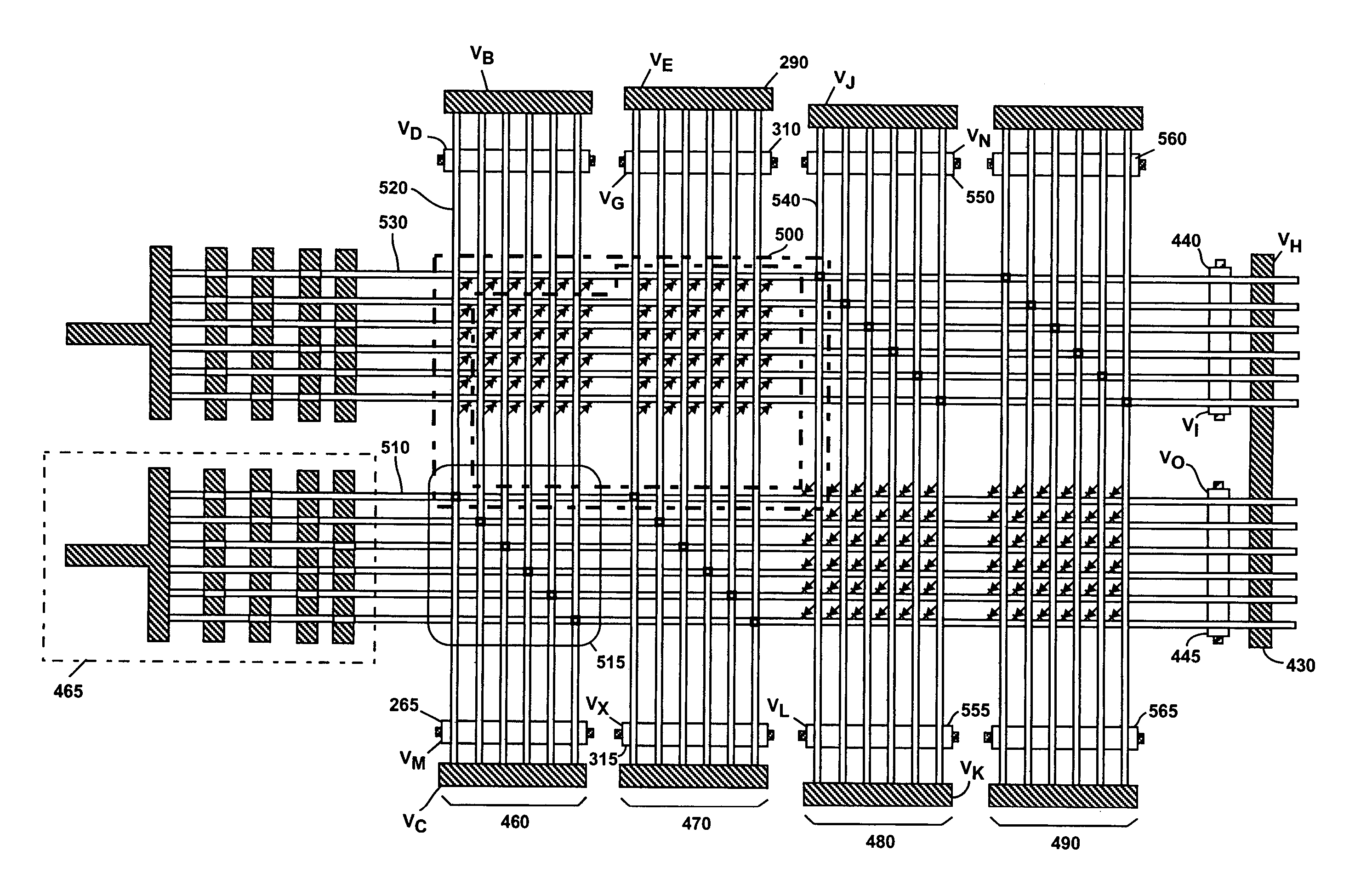
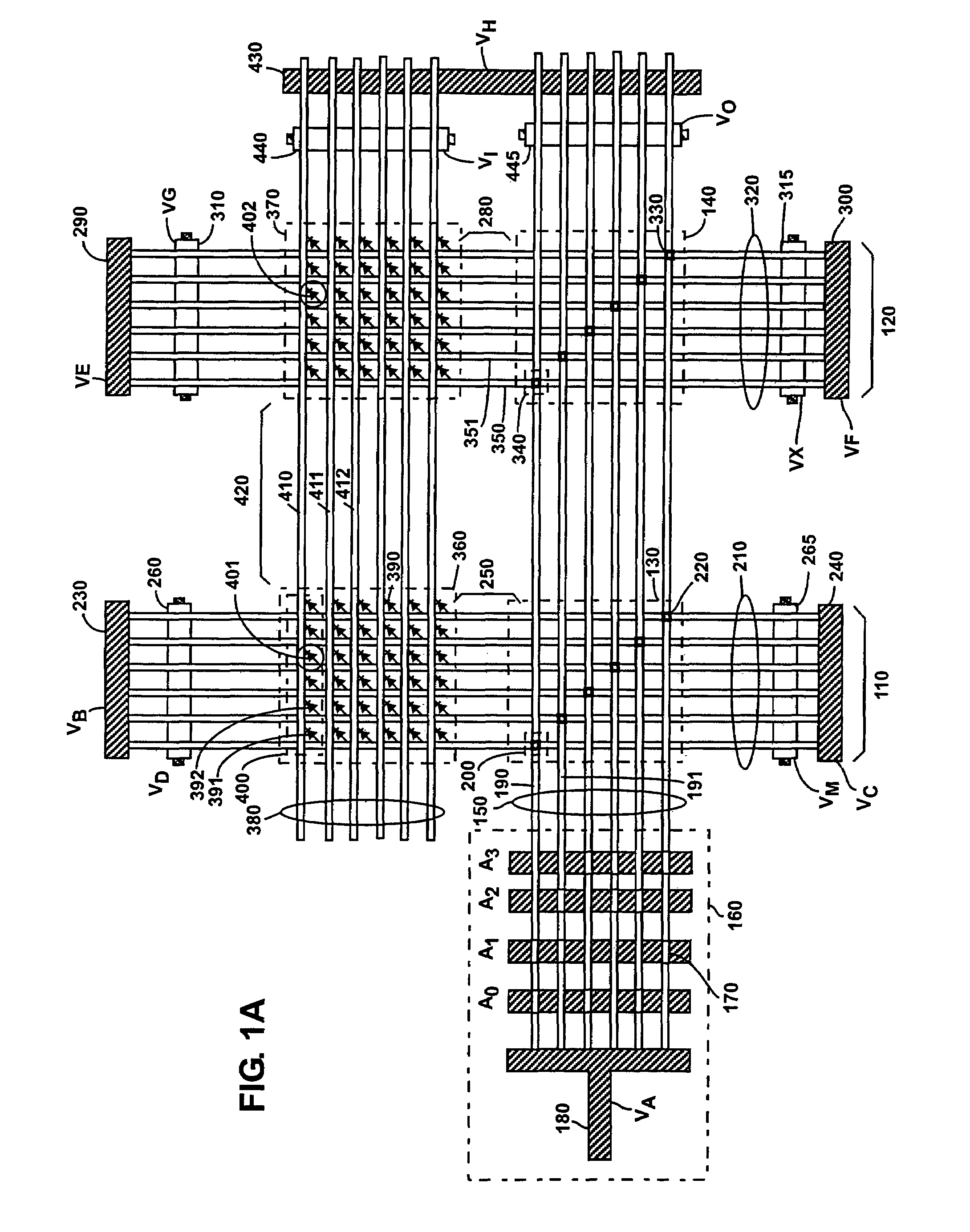
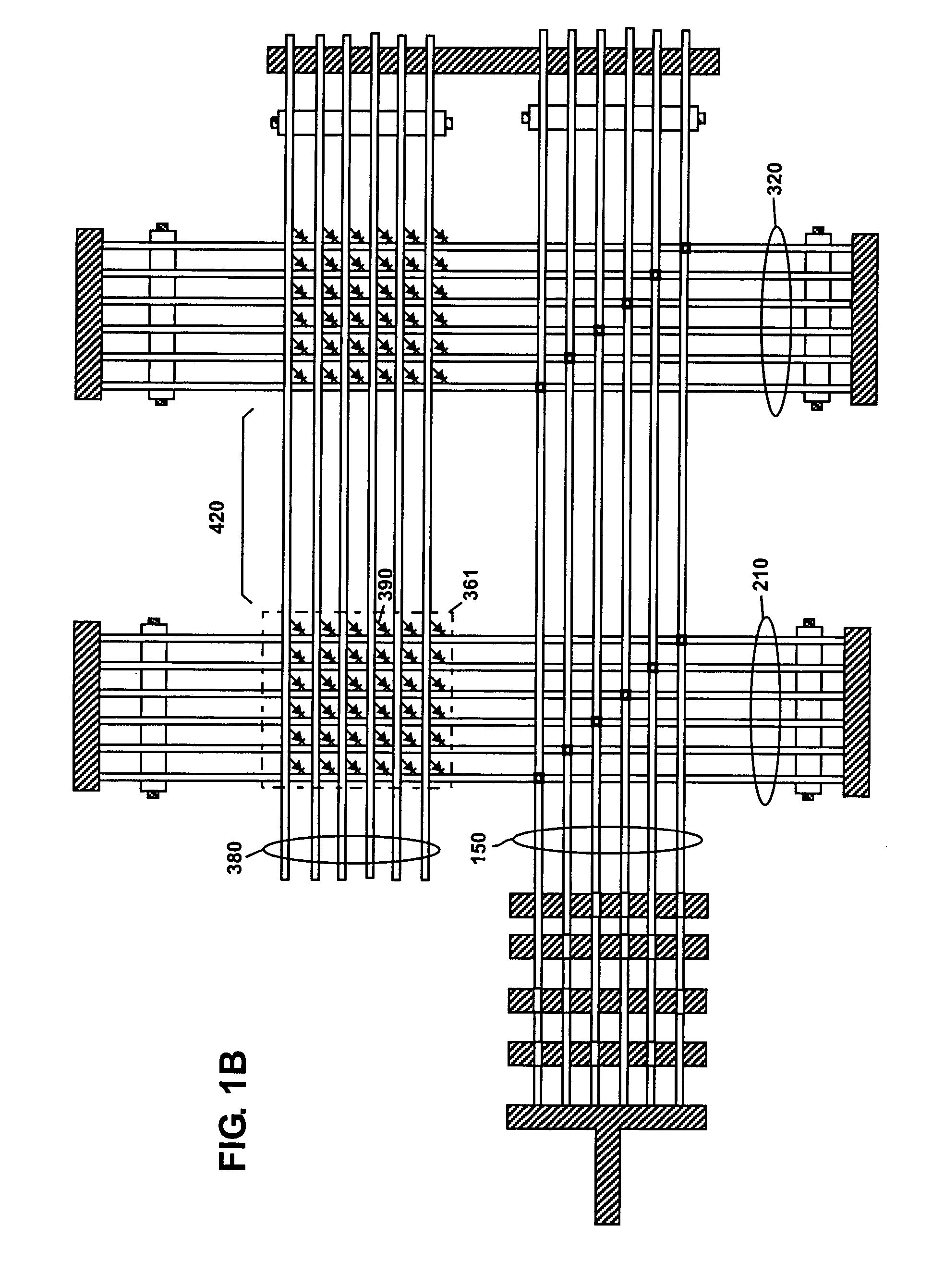
[0065]FIG. 1A discloses a single-plane sublithographic PLA made with nanoscale wires.

[0066]Nanoscale wires 150, 210, 320 and 380 can be grown to controlled dimensions on the nanometer scale using seed catalysts (e.g. gold balls) to define their diameter. Flow techniques can be used to align a set of nanoscale wires 150, 210, 320 or 380 into a single orientation, close pack the nanoscale wires, and transfer the nanoscale wires onto a surface. This step can be rotated and repeated to get multiple layers of nanoscale wires such as crossed nanowires (e.g. 150, 380 cross 210, 320) for building a crossbar array or memory core. By controlling the mix of elements in the environment during growth, nanoscale wires are doped to create controllable regions 170, 220 to control nanoscale wires' electrical properties. See, Y. Cui, X. Duan, J. Hu, and C. M. Lieber, Doping and electrical transport in silicon nanowires, Journal of Physical Chemistry B, 104(22):5213-5216, Jun. 8, 2000.

[0067]The doping...


PUM


Abstract

An apparatus and methods for interconnecting a plurality of nanoscale programmable logic array (PLA) clusters are disclosed. The appartus allows PLA clusters to be built at nanoscale dimensions, signal restoration to occur at the nanoscale, and interconnection between PLA clusters to be performed with nanoscale wiring. The nanoscale PLA, restoration, and interconnect arrangements can be constructed without using lithographic patterning to produce the nanoscale feature sizes and wire pitches. The nanoscale interconnection of the plurality of nanoscale PLA clusters can implement any logic function or any finite state machine. The nanoscale interconnect allows Manhattan (X,Y grid) routing between arbitrary nanoscale PLA clusters. The methods teach how to interconnect nanoscale PLAs with nanoscale interconnect and how to build arbitrary logic with nanoscale feature sizes without using lithography to pattern the nanoscale features.

Description

CROSS-REFERENCE TO RELATED APPLICATIONS[0001]This application claims the benefit of U.S. provisional Patent Application Ser. No. 60 / 592,514, filed Jul. 29, 2004 for “Implementation of Computation Note 27: Working Notes on Interconnected NanoPLA Clusters” by Andre' DeHon, U.S. provisional Patent Application Ser. No. 60 / 610,840, filed Sep. 17, 2004 for “Design of Programmable Interconnect for Sublithographic Programmable Logic Arrays” by Andre' DeHon, U.S. provisional Patent Application Ser. No. 60 / 615,991, filed Oct. 5, 2004 for “Design of Programmable Interconnect for Sublithographic Programmable Logic Arrays” by Andre' DeHon, and U.S. provisional Patent Application Ser. No. 60 / 637,515, filed Dec. 20, 2004 for “Design of Programmable Interconnect for Sublithographic Programmable Logic Arrays” by Andre' DeHon, the disclosure of all of which is incorporated herein by reference in its entirety.[0002]This application is a continuation in part of U.S. patent application Ser. No. 10 / 856,1...

Claims


Application Information

Patent Timeline
Patent Type & Authority Patents(United States)
IPC IPC(8): H01L25/00H03K19/177
CPCH03K19/17728H03K19/17796H03K19/1778H03K19/17736
Inventor DEHON, ANDRE M.
Owner CALIFORNIA INST OF TECH
Why Eureka
Try Eureka