This helps you quickly interpret patents by identifying the three key elements:
Problems solved by technology
Method used
Benefits of technology
Benefits of technology
[0030]In an advantageous development of the invention, the fuse in series with the zener diode is embodied as a fusible resistor. This prevents, in particular, the transistors from being destroyed in the event of overloading of the array.
[0031]The value of the resistor in series with the zener diode preferably lies in the range between 100 ohms and 1000 ohms, so that the required compensating voltages can once again be generated with relatively small currents.
[0032]M
Problems solved by technology
In the case of such LED arrays, on account of the steep U/I characteristic curve of LEDs, even small changes in the forward voltage can bring about a great change in current and thus lead to a considerable deviation of the current intensity in the individual LED chains of the LED array from a predetermined desired current intensity.
This is associated with comparatively high costs since corresponding logistics and stockkeeping are necessary.
Therefore, a change in temperature may lead to a change in the forward voltages.
However, rising accuracy requirements w
Method used
Image
Click on the blue label to locate the original text in one second.
Reading with bidirectional positioning of images and text.
Examples
Example
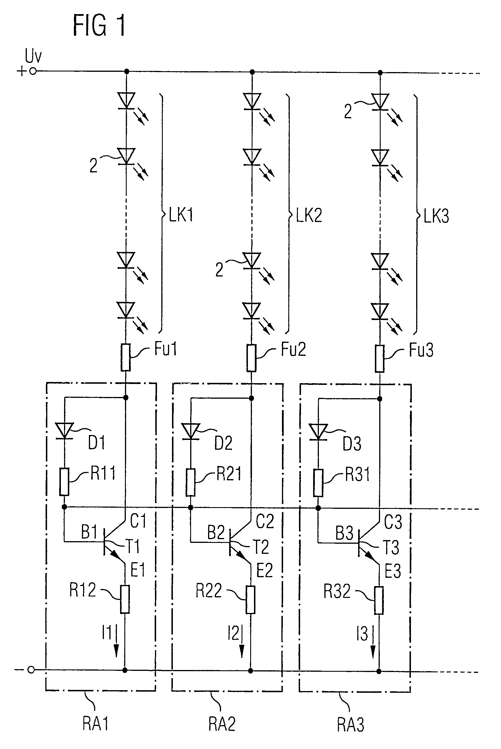
[0060]A further advantage of the first embodiment of the invention or the exemplary embodiment illustrated in FIG. 1 is that a partial current is branched off for regulating purposes in each LED chain LKx. This increases the reliability and stability of the system. When using emitter resistors R12, R22, R32 with a 1% tolerance, the tolerance of the base currents is 2%, with the result that a comparatively high precision of the current distribution is obtained overall.
[0061]As already explained, the circuit arrangement in accordance with FIG. 1 can be extended by any desired number of LED chains in the manner illustrated.
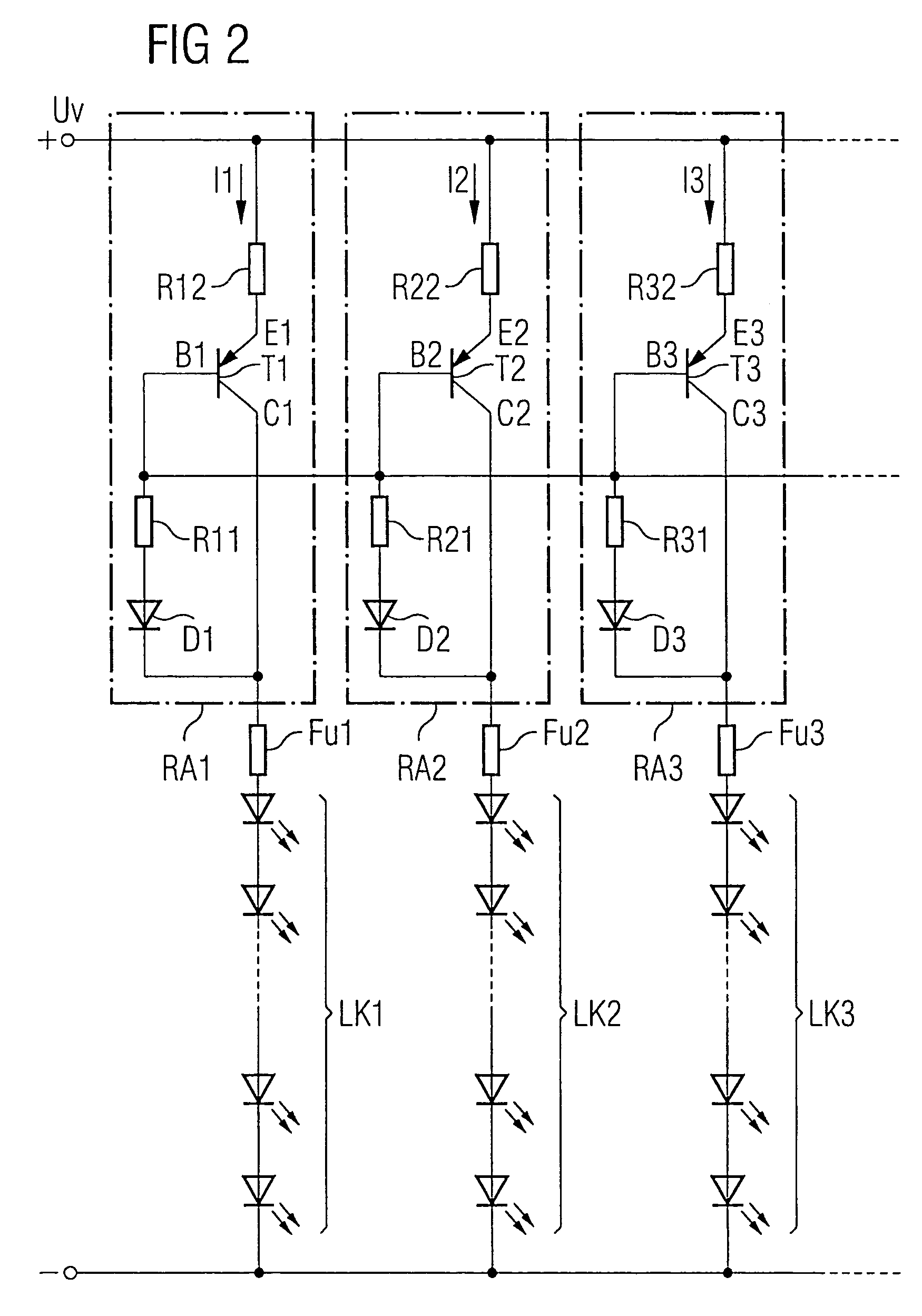
[0062]The circuit shown in FIG. 1 can also be constructed in an analogous manner using pnp transistors. A corresponding second exemplary embodiment of the invention is illustrated in FIG. 2. In this case, the regulating arrangements RA1, RA2, RA3 with the transistors T1, T2, T3, the emitter resistors R12, R22, R32 and the drive circuits comprising the resistors R11, ...
Example
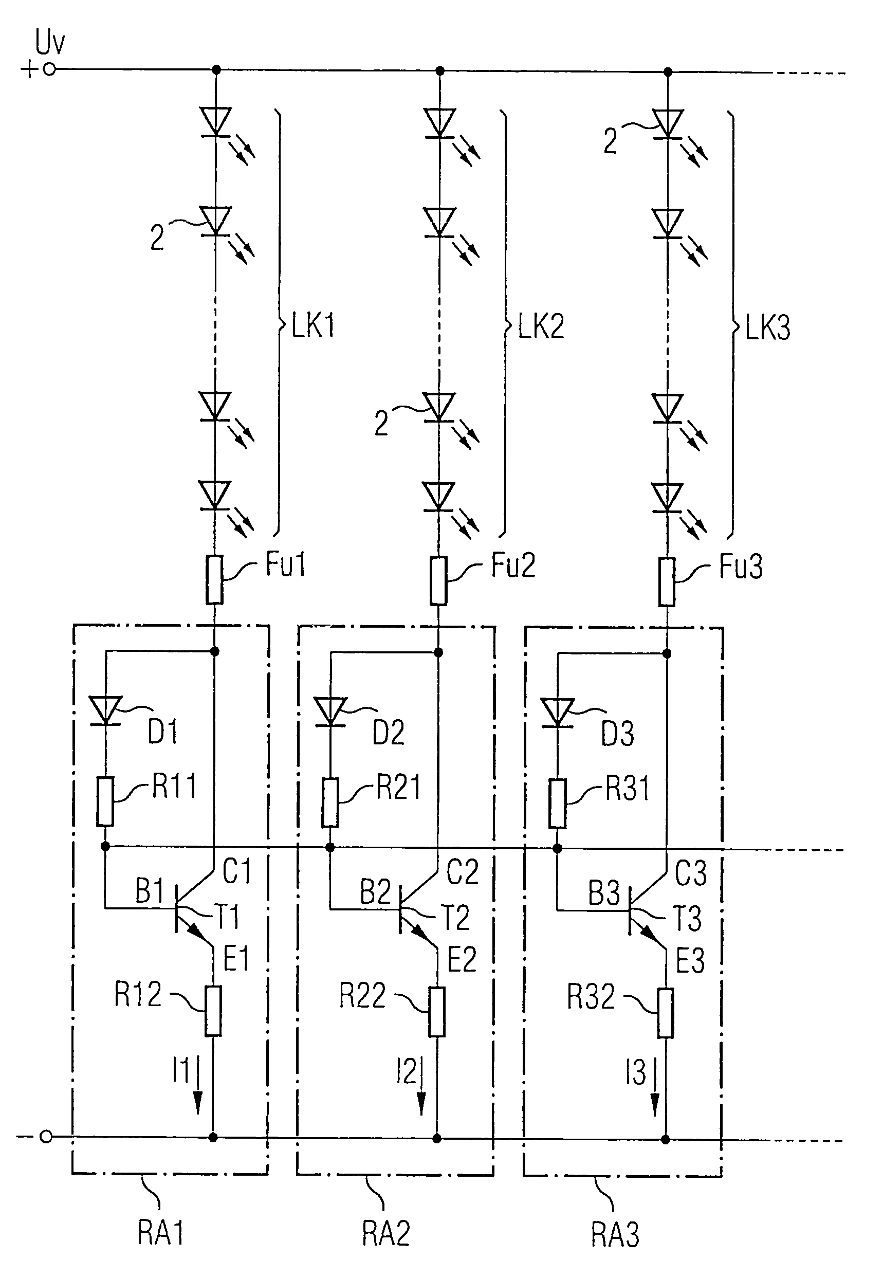
[0066]FIG. 4 shows a fourth exemplary embodiment in accordance with the second embodiment of the invention. As in the case of the exemplary embodiment illustrated in FIG. 1, here as well a plurality of LEDs 2 are in each case connected in series to form LED chains LK1, LK2, LK3 and the LED chains LK1, LK2, LK3 are connected, on the anode side, to the positive pole of a supply voltage and, on the cathode side, via an optional fuse Fu1, Fu2, Fu3, in each case to a regulating arrangement RA1, RA2, RA3.
[0067]The regulating arrangements RA1, RA2, RA3 once again in each case comprise a transistor Tx, the collector terminal Cx of which is connected to the corresponding LED chain LKx. The emitter terminal Ex is in each case connected via an emitter resistor Rx2 to the negative pole of the supply voltage.
[0068]As in the previous exemplary embodiments, the base terminals B1, B2, B3 of the transistors T1, T2, T3 are connected to one another and are thus at the same potential.
[0069]In contrast ...
PUM
Abstract
A circuit arrangement for an LED array having two or more parallel-connected LED chains (LK1, LK2, LK3), in each of which at least one LED (2) is arranged and, when there are two or more LEDs (2), the latter are connected in series. In each case, the anode sides of the LED chains (LK1, LK2, LK3) can be coupled to the positive pole of a supply voltage (Uv) and the cathode sides can be coupled to the negative pole of the supply voltage (Uv). A regulating arrangement (RA1, RA2, RA3) for regulating an intended current distribution between the individual LED chains (LK1, LK2, LK3) is case connected in series with the respective LED chain (LK1, LK2, LK3).
Description
RELATED APPLICATIONS[0001]This is a U.S. national stage of application No. PCT / DE02 / 04329, filed on 26 Nov. 2002.[0002]This patent application claims the priority of German patent application nos. 101 57 645.5 and 102 42 365.2 filed 26 Nov. 2001 and 12 Sep. 2002, respectively, the disclosure content of which is hereby incorporated by reference.FIELD OF THE INVENTION[0003]The present invention relates to a circuit arrangement for an LED array, in particular for a light signal device, having two or more parallel-connected LED chains, in each of which at least one LED (light emitting diode) is arranged, and, when there are two or more LEDs, the latter are connected in series. The anode sides of the LED chains can in each case be coupled to the positive pole of a supply voltage and the cathode sides can in each case be coupled to the negative pole of the supply voltage.BACKGROUND OF THE INVENTION[0004]In the case of such LED arrays, on account of the steep U / I characteristic curve of LE...
Claims
Application Information
Patent Timeline
Application Date:The date an application was filed.
Publication Date:The date a patent or application was officially published.
First Publication Date:The earliest publication date of a patent with the same application number.
Issue Date:Publication date of the patent grant document.
PCT Entry Date:The Entry date of PCT National Phase.
Estimated Expiry Date:The statutory expiry date of a patent right according to the Patent Law, and it is the longest term of protection that the patent right can achieve without the termination of the patent right due to other reasons(Term extension factor has been taken into account ).
Invalid Date:Actual expiry date is based on effective date or publication date of legal transaction data of invalid patent.

