Optical metrology on patterned samples

a technology of optical metrology and patterned samples, applied in the field of metals, can solve the problems of computational cost still being orders of magnitude less than the computational cost of generating these multiple sets of coefficients, and achieve the effect of accurately measuring attributes and eliminating the need for complex and resource-intensive computation

Active Publication Date: 2008-01-22
KLA TENCOR TECH CORP
View PDF8 Cites 51 Cited by
  • Summary
  • Abstract
  • Description
  • Claims
  • Application Information

AI Technical Summary

Benefits of technology

[0029]The invention provides a system and method for accurately measuring attributes (e.g., thickness, index of refraction, coefficient of extinction, surface roughness, composition) of a thin film(s) formed on a patterned base layer by creating an empirical optical model for the test sample. By incorporating the empirical model into an optical metrology measurement technique, the invention beneficially eliminates the need for the complex and resource-intensive computation of accurate theoretical models of the film stack.

Problems solved by technology

However, the computational cost of generating these multiple sets of coefficients is still orders of magnitude less than the computational cost of actually solving the theoretical equations for a grating-based thin film stack.

Method used


Image

  • Optical metrology on patterned samples
  • Optical metrology on patterned samples
  • Optical metrology on patterned samples

Examples


Embodiment Construction

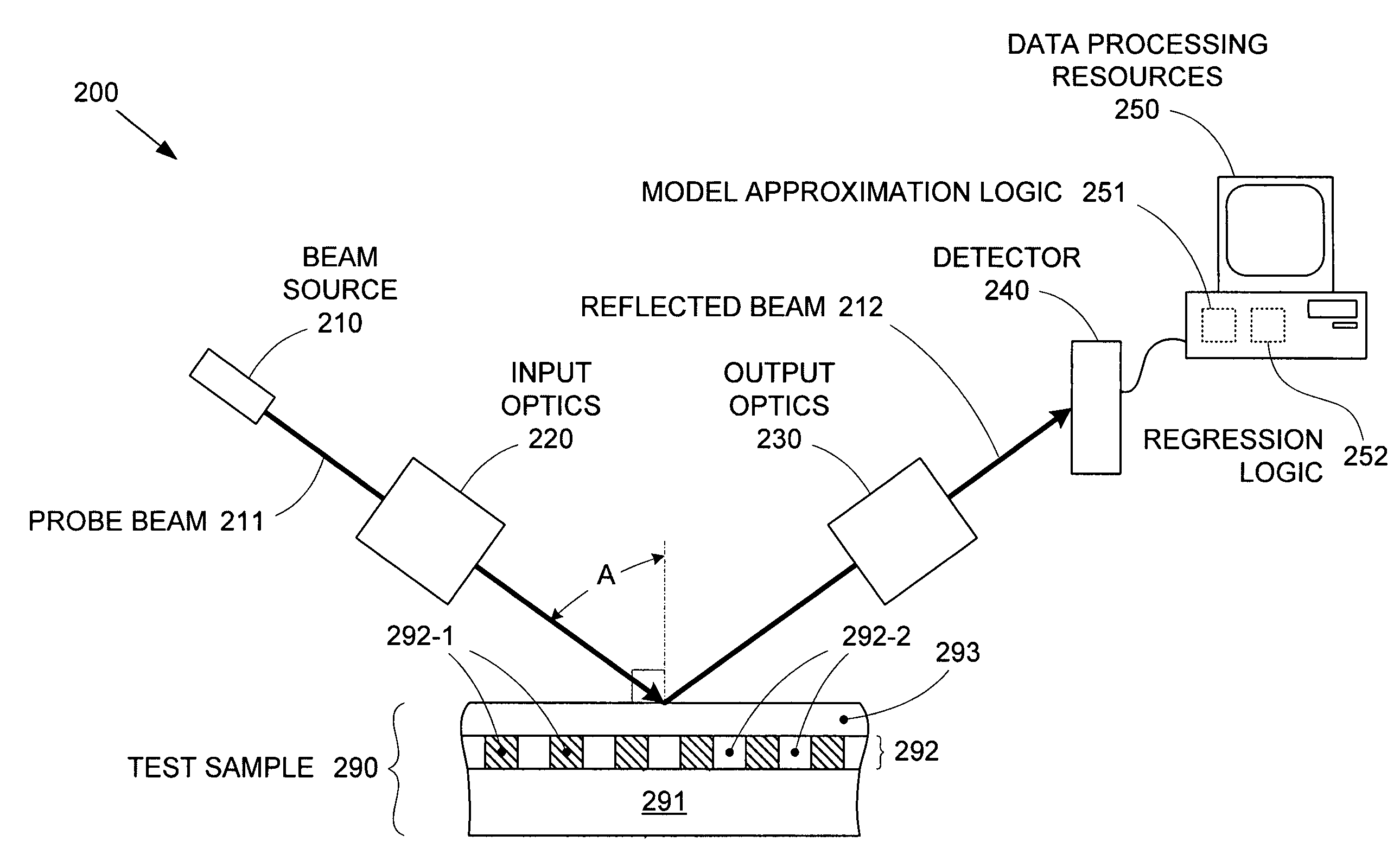
[0049]FIG. 2 shows an optical metrology system 200 for determining values for one or more AOIs (i.e., attributes of interest, such as thickness, index of refraction, roughness, and composition, among others) of a test sample 290, according to an embodiment of the invention. Optical metrology system 200 includes a beam source 210, input optics 220, output optics 230, a detector 240, and data processing resources 250. For exemplary purposes, test sample 290 includes a patterned base layer 292 formed on a substrate 291, and a thin film 293 formed on patterned base layer 292. Patterned base layer 292 includes a series of lines 292-1 (e.g., metal lines) formed in a base material 292-2. Note that while patterned base layer 292 is depicted as a patterned base layer for exemplary purposes, patterned base layer 292 can include any type of patterning. Note further that thin film 293 can be made up of any number of material layers.

[0050]To perform a measurement operation, a probe beam 211 gene...


PUM


Abstract

An optical metrology system includes model approximation logic for generating an optical model based on experimental data. By eliminating theoretical model generation, in which the fundamental equations of a test sample must be solved, the model approximation logic significantly reduces the computational requirements of the metrology system when measuring films formed on patterned base layers. The experimental model can be created by selecting an expected mathematical form for the final model, gathering experimental data, and compiling a lookup model. The lookup model can include the actual measurement data sorted by output (attribute) value, or can include “grating factors” that represent compensation factors that, when applied to standard monolithic model equations, compensate for the optical effects of grating layers.

Description

BACKGROUND OF THE INVENTION[0001]1. Field of the Invention[0002]The invention relates to the field of metrology, and in particular to computationally efficient optical metrology systems.[0003]2. Related Art[0004]Optical metrology tools (such as ellipsometry tools or reflectometry tools) determine the attributes of thin films in integrated circuits (ICs) by reflecting a probe beam of light off of the thin films. Data measurements from the reflected beam are collected and compared to an optical model of the thin films and any interfacing structures to generate values for the thin film attribute(s) of interest.[0005]Typically, optical metrology is performed on thin films formed on predetermined target regions of a wafer. Those target regions have historically included thin films formed on uniform (monolithic) base layers. However, as device geometries decrease and IC yield and performance requirements become more sensitive to process defects, monolithic targets (i.e., targets located o...

Claims


Application Information

Patent Timeline
Patent Type & Authority Patents(United States)
IPC IPC(8): G01J4/00G01B11/00
CPCG01N21/211G01N21/8422
Inventor POSLAVSKY, LEONIDYGARTUA, CARLOS L.
Owner KLA TENCOR TECH CORP
Why Eureka
Try Eureka