
Thin film transistor array substrate and repairing method thereof

a technology of thin film transistors and array substrates, applied in non-linear optics, instruments, optics, etc., can solve problems such as defective pixels, failure of storage capacitors, and inability to normally function pixels, so as to eliminate abnormal display issues of pixels and improve manufacturing yields

Active Publication Date: 2008-02-12
AU OPTRONICS CORP
View PDF10 Cites 2 Cited by
  • Summary
  • Abstract
  • Description
  • Claims
  • Application Information

AI Technical Summary

Benefits of technology

[0011]Accordingly, the present invention is directed to a TFT array substrate to prevent the abnormally displaying issue of the pixel resulting from process defects, and to enhance manufacturing yields.
[0012]The present invention is also directed to a repairing method of a TFT array substrate to repair the defective pixel of the TFT array substrate, and to enhance manufacturing yields of the TFT array substrate.
[0028]Accordingly, the TFT array substrate and the repairing method thereof repair different types of defective pixels by the design of the conductive line and the connection part of the top electrode. As a result, the defective pixels can normally function. The TFT array substrate and the repairing method thereof effectively eliminate the abnormally displaying issue of the pixel resulting from process defects and improve the manufacturing yields.

Problems solved by technology

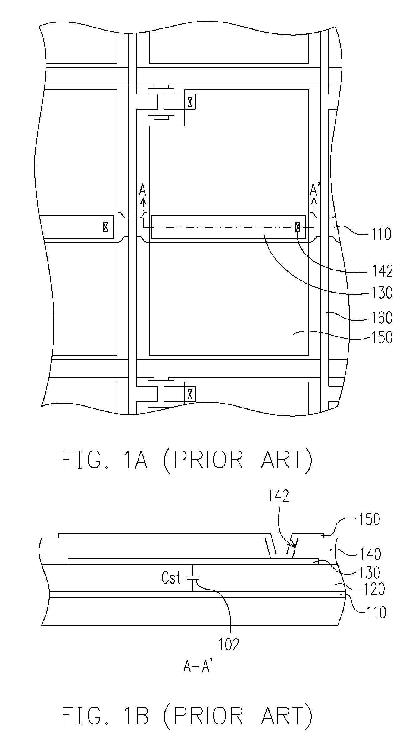
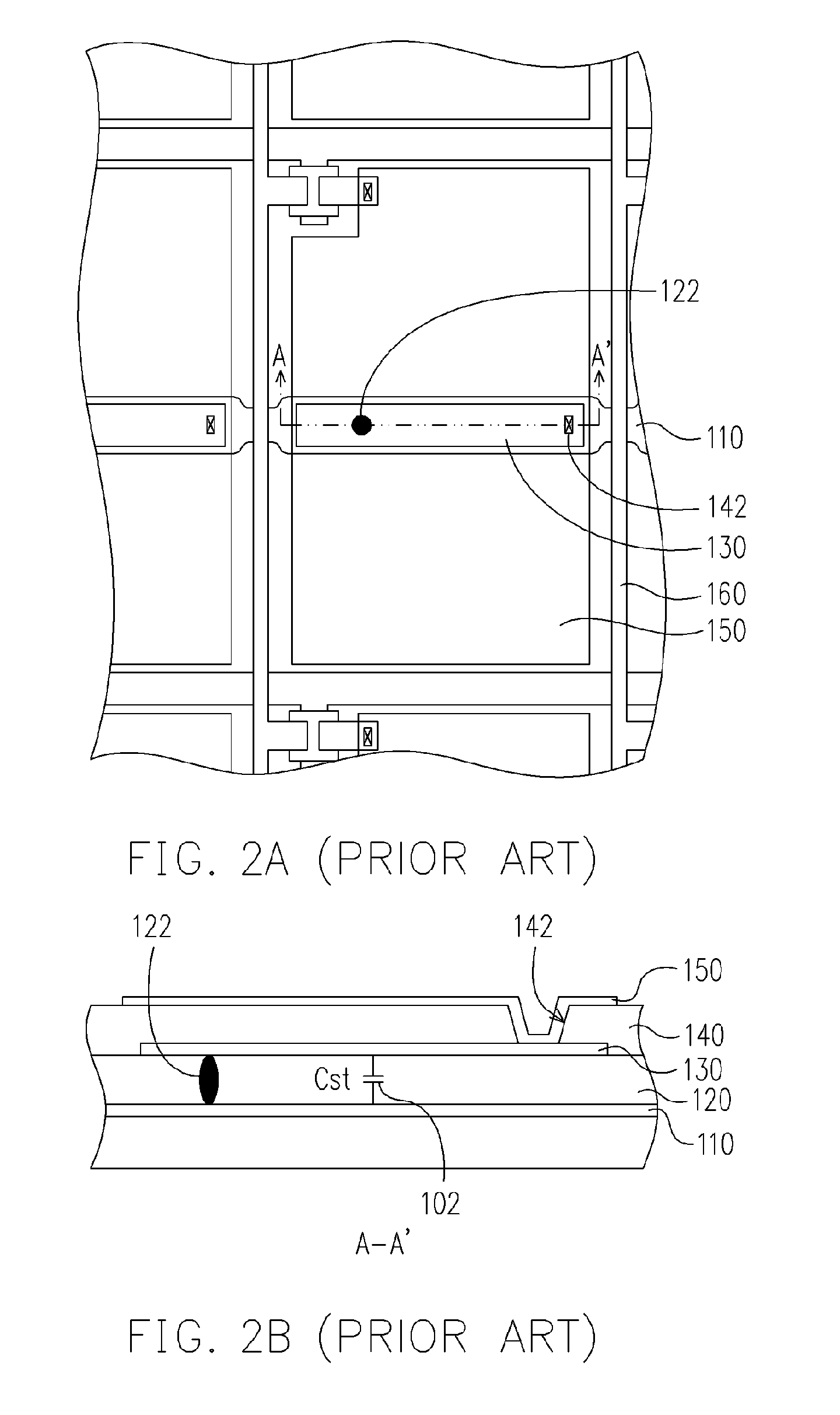
During forming the prior art TFT array, failures of storage capacitors may occur due to defects or other reasons.
Such failures will result in defective pixels.
No matter what situation described above, the pixel cannot normally function, and the display quality of the LCD will be affected.

Method used


Image

  • Thin film transistor array substrate and repairing method thereof
  • Thin film transistor array substrate and repairing method thereof
  • Thin film transistor array substrate and repairing method thereof

Examples


Embodiment Construction

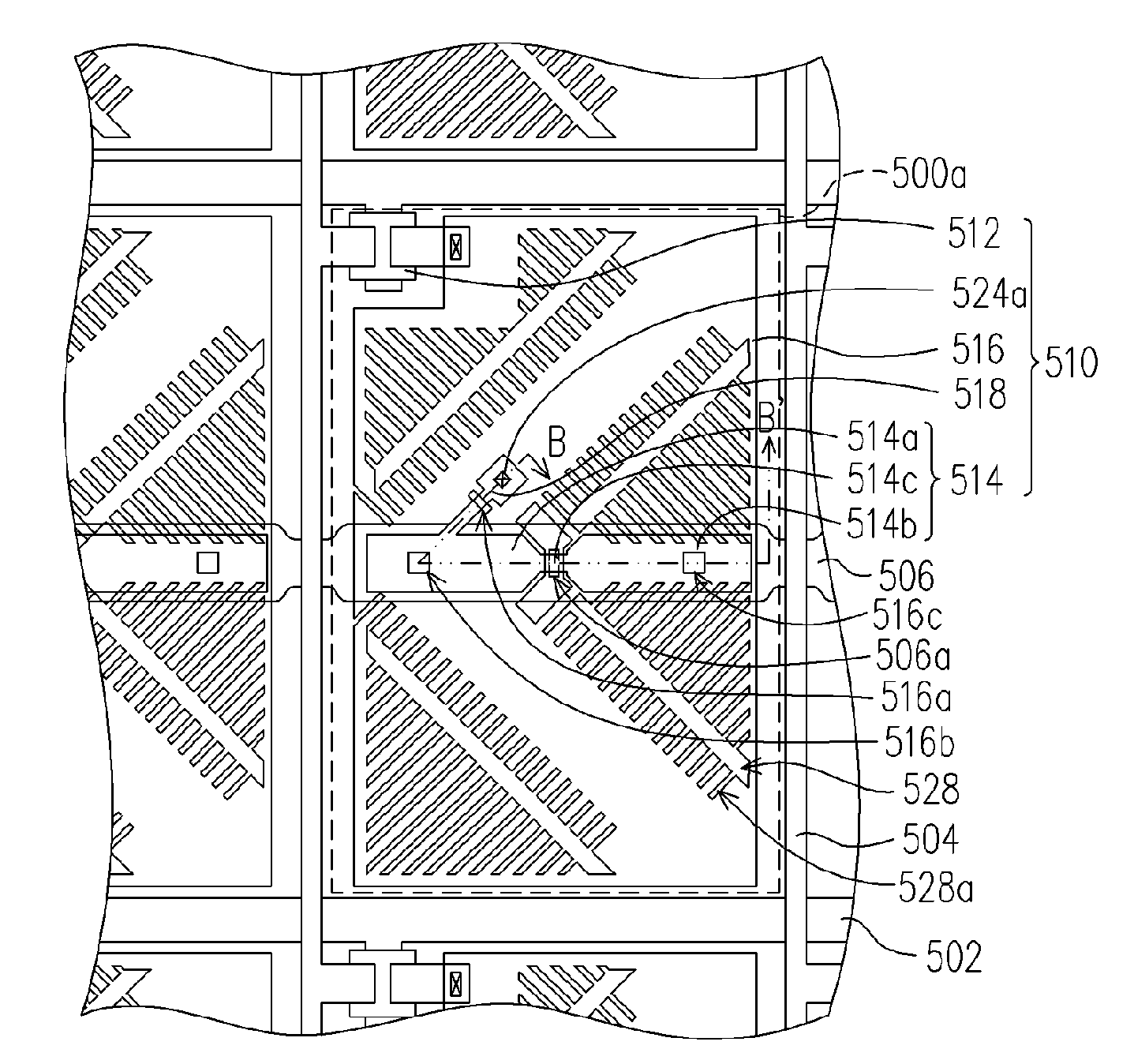
[0048]FIG. 5A is a regional top view of a TFT array substrate according to an embodiment of the present invention. FIG. 5B is a cross-sectional view along B-B′ shown in FIG. 5A. The TFT array substrate is adapted for a Multi-Domain Vertical Alignment (MVA) LCD panel, for example. Referring to FIGS. 5A and 5B, the substrate 500 can be, for example, a glass substrate. A plurality of scan lines 502 and a plurality of data lines 504 are disposed over the substrate 500, for example, and define a plurality of pixel areas 500a on the substrate 500. In addition, a plurality of common lines 506 is disposed over the substrate 500. The common lines 506 and the scan lines 502 can be formed in a same process, and the material is for example Cr, Al, or other metals with good conductivity. Each of the common lines 506 is disposed in the pixel area 500a corresponding thereto.

[0049]Referring to FIGS. 5A and 5B, each pixel area 500a comprises a pixel 510, for example. The pixel 510 comprises a TFT 51...


PUM

PropertyMeasurementUnit
areasaaaaaaaaaa
conductiveaaaaaaaaaa
parasitic capacitanceaaaaaaaaaa

Abstract

A thin film transistor array substrate and a repairing method thereof are provided. The thin film transistor array substrate comprises a substrate, plural scan lines, plural data lines, plural common lines, and plural pixels. The scan lines and the data lines are disposed over the substrate and define plural pixel areas. Each pixel is disposed in one of the pixel areas corresponding thereto. Each pixel comprises a thin film transistor, a pixel electrode, a top electrode, and a conductive line. In each pixel, the thin film transistor is coupled to the corresponding scan line and the corresponding data line, and the pixel electrode is disposed over the corresponding common line. Furthermore, the top electrode is disposed between the corresponding pixel electrode and common line, and the conductive line is disposed out of the corresponding common line and coupled between the corresponding top electrode and pixel electrode.

Description

CROSS-REFERENCE TO RELATED APPLICATION[0001]This application claims the priority benefit of Taiwan application serial no. 94100331, filed on Jan. 6, 2005.BACKGROUND OF THE INVENTION[0002]1. Field of the Invention[0003]The present invention relates to an active device array substrate and a repairing method thereof, and more particularly, to a thin film transistor array substrate and a repairing method thereof.[0004]2. Description of the Related Art[0005]A thin film transistor liquid crystal display (TFT LCD) mainly comprises a TFT array substrate, a color filter array substrate, and a liquid crystal layer. Wherein, the TFT array substrate is composed of a plurality of TFT arrays and pixel electrodes corresponding to each of the TFTs. A TFT serves as a switch of a pixel. In order to control the pixels, the scan lines and the data lines coupled to the TFTs are used to select a specific pixel. By applying a proper operational voltage, the data corresponding to the pixel can be displayed...

Claims


Application Information

Patent Timeline
Patent Type & Authority Patents(United States)
IPC IPC(8): G02F1/1333G02F1/136
CPCG02F1/1343G02F1/136213G02F1/136259
Inventor HUANG, WEI-KAICHEN, YI-JENTSAI, CHEN-SHUNWANG, CHIUNG-PIN
Owner AU OPTRONICS CORP
Learn More