Apparatus and method for connecting optical waveguides
a technology of optical waveguides and alignment methods, applied in the direction of optical waveguide light guides, optical elements, instruments, etc., can solve the problems of significant transmission loss, low precision of optical axis alignment between components, and inability to observe external light propagating through materials, etc., to increase the propagation loss of light and low precision of optical axis alignmen
- Summary
- Abstract
- Description
- Claims
- Application Information
AI Technical Summary
Benefits of technology
Problems solved by technology
Method used
Image
Examples
first modified embodiment
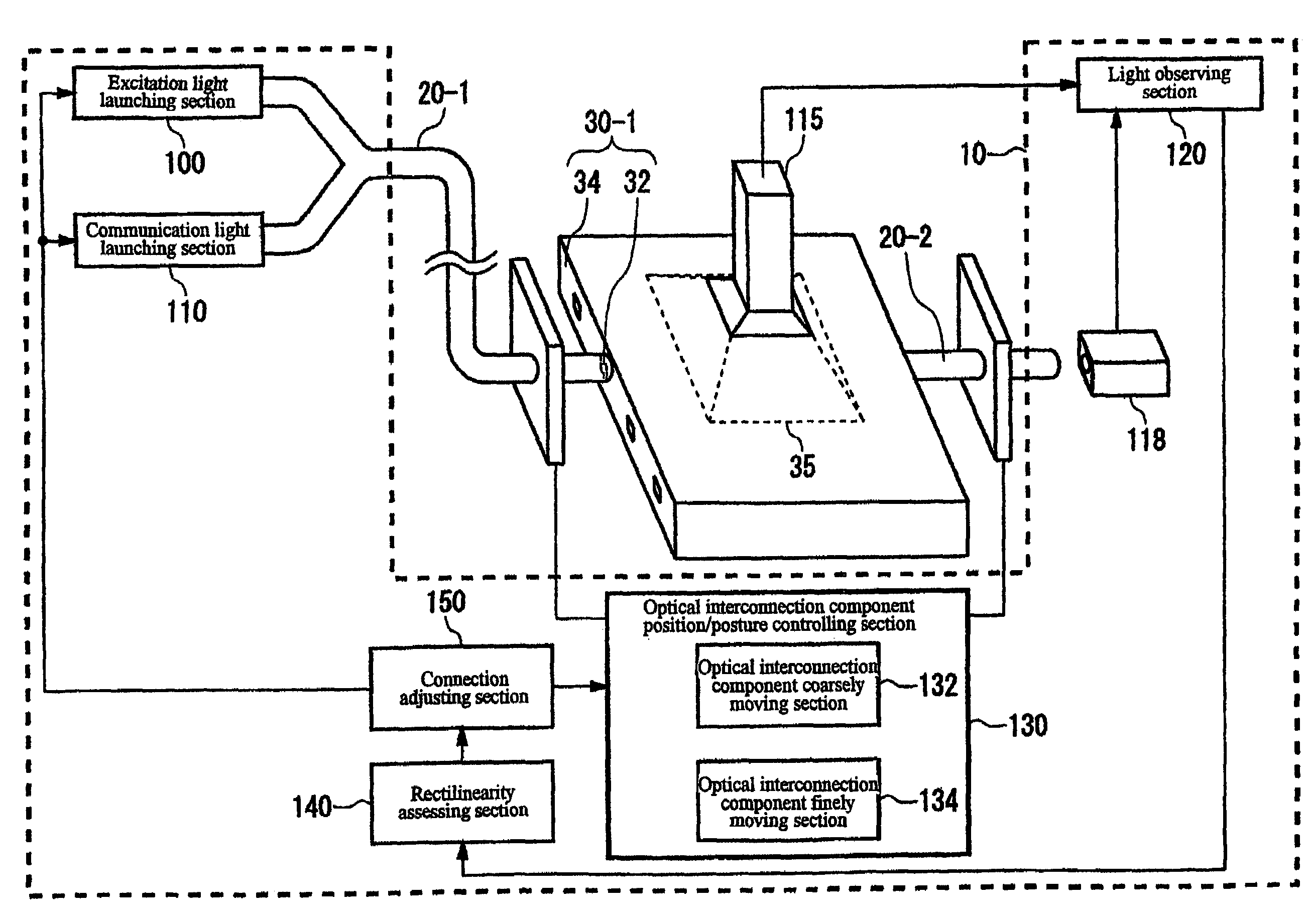
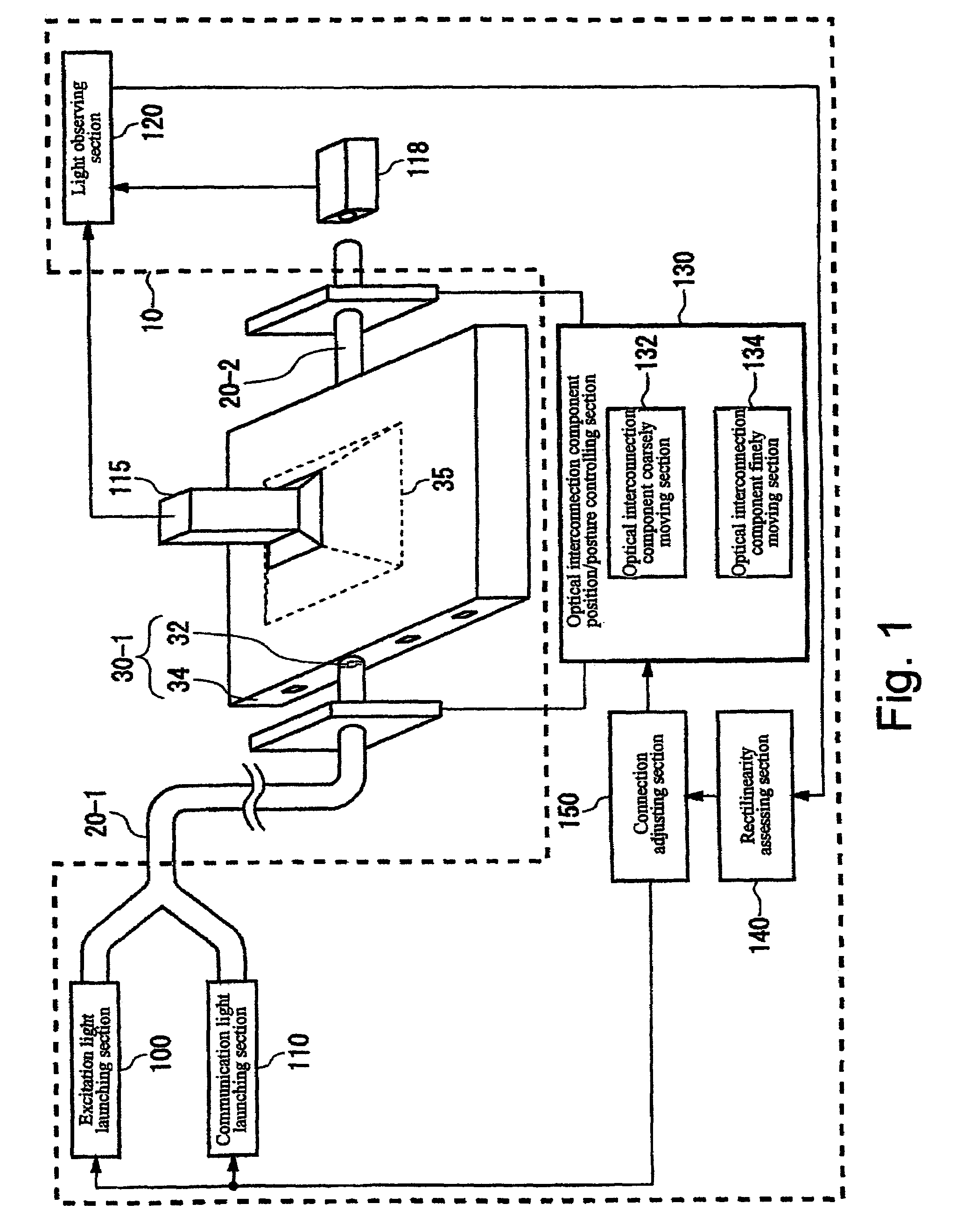
[0076]FIG. 11 shows an arrangement of the aligner 10 according to a According to this modified embodiment, unlike the arrangement shown in FIG. 1, the optical fiber 20-1 is connected to the camera 115. Here, the camera 115 is a device that measures the intensity of the fluorescent light emitted from a point in a plane, such as a photodiode. Preferably, the camera 115 is placed on a normal line drawn to the surface of the waveguide substrate 30-1 and intersecting with the line of the light launched into the waveguide in the waveguide substrate 30-1. Furthermore, preferably, even if the optical fiber 20-1 moves vertically with respect to the plane of the waveguide substrate 30-1, the camera 115 does not move and keeps the distance from the waveguide substrate 30-1 at an appropriate distance for measuring the intensity of the fluorescent light.
[0077]For example, as the optical interconnection component position / posture controlling section 130 moves the optical fiber 20-1 horizontally ...
second modified embodiment
[0079]FIG. 12 shows an arrangement of the aligner 10 according to a The aligner 10 comprises a reflection film 40, the excitation light launching section 100, the light observing section 120, a light receiving element 125, the optical interconnection component position / posture controlling section 130 and the connection adjusting section 150. According to this modified embodiment, the optical fiber 20-1 is cut into two sections, and a lens and a prism are disposed between the two optical fiber sections. In addition, the reflection film 40 is formed on the reflection surface of the prism. For example, the reflection film 40 may be a multi-layer reflection film using the Bragg reflection. In this case, the reflection film has a reflection wavelength equal to the wavelength of the fluorescent light emitted by the waveguide material.
[0080]The excitation light launching section 100 launches the excitation light that causes the waveguide in the waveguide substrate 30-1 to emit fluorescent...
third modified embodiment
[0084]FIG. 13 shows an arrangement of the aligner 10 according to a The aligner 10 comprises the excitation light launching section 100, the communication light launching section 110, the light observing section 120, the optical interconnection component position / posture controlling section 130, the rectilinearly assessing section 140 and the connection adjusting section 150. Unlike the aligner 10 shown in FIG. 1, the aligner 10 according to this modified embodiment is intended to align the waveguide substrate 30-1, which is a first waveguide, and a waveguide substrate 30-2 longer than the waveguide substrate 30-1, which is a second waveguide, that are connected in series with the optical fiber 20-1.
[0085]The excitation light launching section 100 launches the excitation light into one end of the waveguide substrate 30-1 via the optical fiber 20-1. The communication light launching section 110 launches the light for optical communications into the waveguide in the waveguide substra...
PUM
 Abstract
Description
Claims
Application Information


