
Wavelength conversion devices

a conversion device and wavelength technology, applied in the direction of instruments, light demodulation, optical waveguide light guides, etc., can solve the problems of deteriorating coupling efficiency, increasing and reducing the coupling efficiency of optical fibers outside the device, so as to increase the propagation loss of light and the harmonic output is higher

Active Publication Date: 2009-12-15
NGK INSULATORS LTD
View PDF14 Cites 0 Cited by
  • Summary
  • Abstract
  • Description
  • Claims
  • Application Information

AI Technical Summary

Benefits of technology

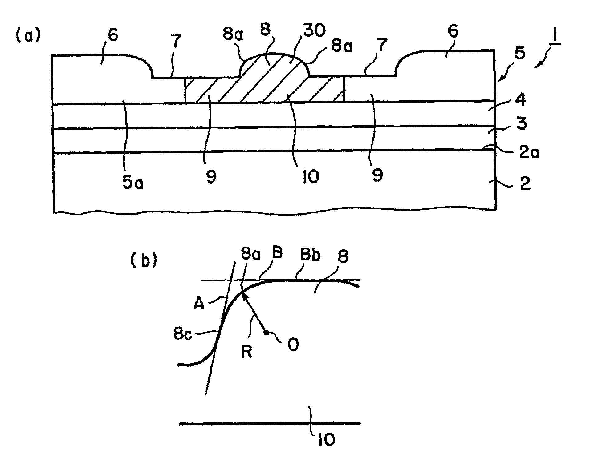
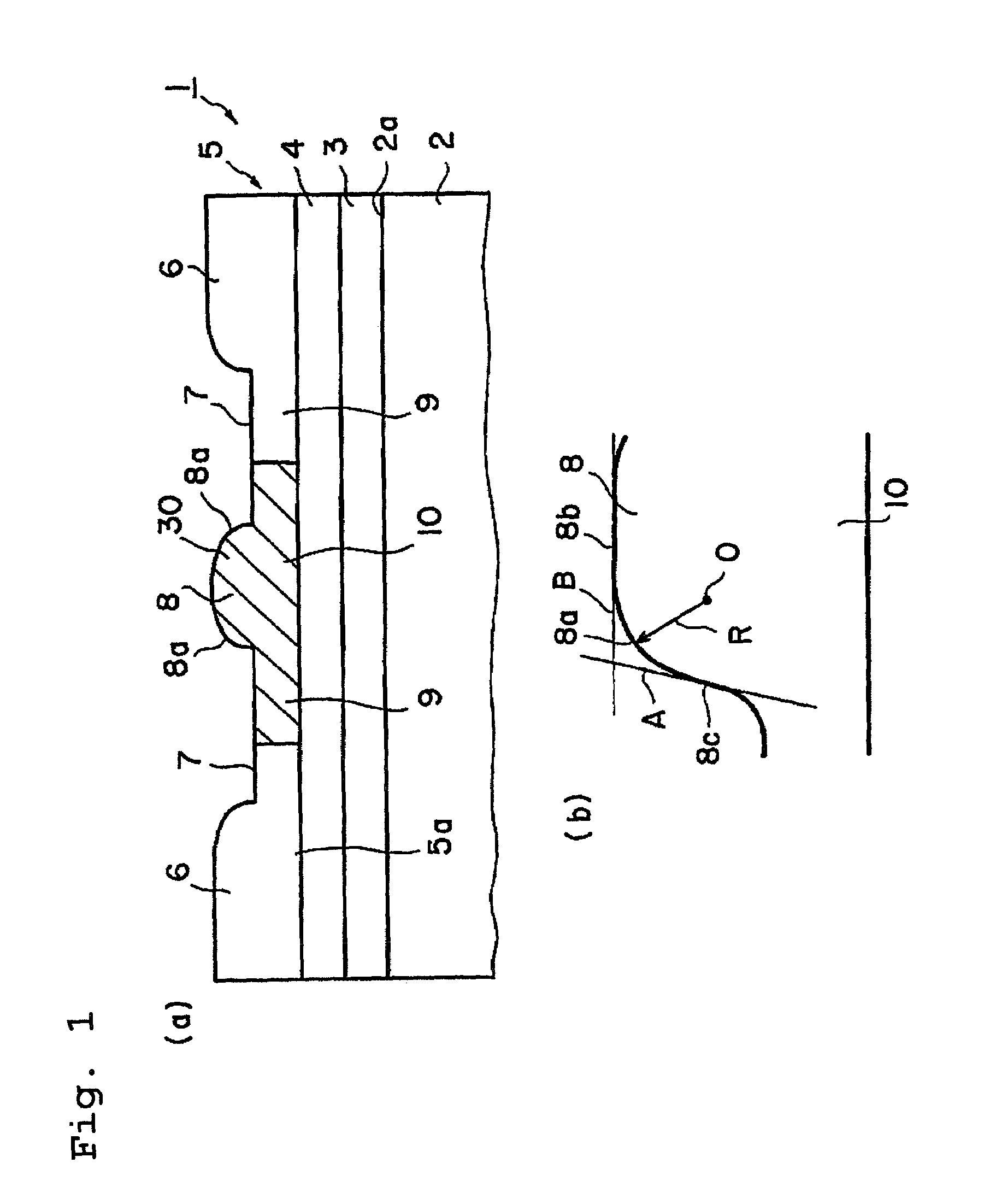
The present invention is about improving the generation efficiency of higher harmonics in a wavelength conversion device that includes a ridge optical waveguide and a periodic domain inversion structure. The inventors found that the asymmetry distorted propagating mode caused deteriorating coupling efficiency and increasing propagation loss. To address this issue, the inventors polished the surface of the ridge area, particularly the edge areas, to process them into R-faces. After confirming the improved shape of the propagating mode, the inventors found that the higher harmonic output was remarkably enhanced in comparison to the case before the R-faces were formed.

Problems solved by technology

However, in the case of forming the ridge optical waveguide in the area where the periodic domain inversion structure is formed and making the fundamental wave incident onto the waveguide, the coupling efficiency to, for example, an optical fiber outside the device decreased in many cases; and a tendency was observed which increased the propagation loss of light.
The inventors found that this asymmetry distorted propagating mode becomes a cause of deteriorating the coupling efficiency and increasing the propagation loss.

Method used


Image

  • Wavelength conversion devices
  • Wavelength conversion devices
  • Wavelength conversion devices

Examples


examples

[0039]The wavelength conversion device 1 illustrated in FIG. 1 was manufactured. Concretely, a comb-shaped periodic electrode with the period of 6.53 μm was formed on an MgO 5% doped lithium niobate-5 degree off-cut Y substrate of 0.5 mm thick, by photolithography. An electrode membrane was formed over the entire surface of the back face of the substrate; thereafter, a pulse voltage was applied to form a periodic domain inversion structure. After forming the periodic domain inversion, a SiO2 under clad 4 of 0.6 μm thick was formed by the sputtering.

[0040]An adhesive was applied to a non-doped lithium niobate substrate 2 of 0.5 mm thick, to which was stuck the above MgO doped lithium niobate substrate. The surface of the MgO doped lithium niobate substrate was abraded and polished until the thickness thereof reached 3.8 μm.

[0041]Next, a ridge waveguide was formed by the laser abrasion, in a manner that the center of the waveguide is located 10 μm distant from the front end of the per...


PUM

PropertyMeasurementUnit
widthaaaaaaaaaa
curvature radiusaaaaaaaaaa

Abstract

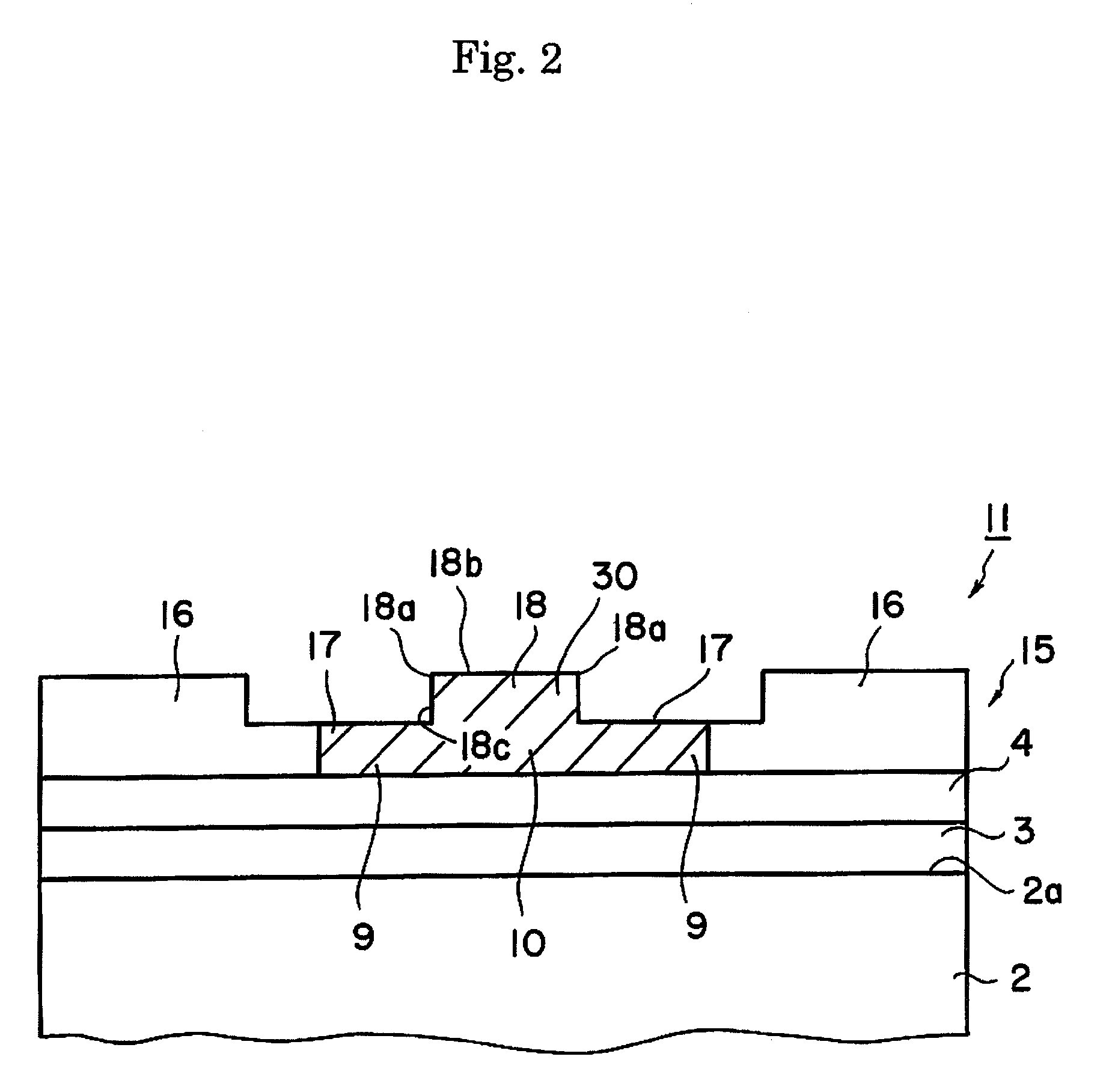
A wavelength conversion device is provided having a ridge optical waveguide and a periodic domain inversion structure formed in the waveguide. The optical waveguide has side wall faces, an upper face and edge areas formed between the upper face and the side wall face, respectively. R-faces are formed on the edge areas.

Description

[0001]This application claims the benefit of Japanese Patent Application P 2007-58369 filed on Mar. 8, 2007, the entirety of which is incorporated by reference.BACKGROUND OF THE INVENTION[0002]1. Field of the Invention[0003]The present invention relates to a wavelength conversion device.[0004]2. Related Art[0005]An optical frequency modulator utilizing the surface acoustic wave, an optical wavelength conversion device utilizing the polarization inversion of non-linear domain and so forth can be realized by periodically forming the domain inversion structure wherein the ferroelectric polarization is forcibly inverted. Especially, if the periodic domain inversion of non-linear optical materials becomes possible, a high-efficiency wavelength conversion device can be manufactured; and to convert a solid state laser beam, for example, by using the above wavelength conversion device will make it possible to build up a small and light short-wavelength light source, which can be applied to ...

Claims


Application Information

Patent Timeline
Patent Type & Authority Patents(United States)
IPC IPC(8): G02F2/02
CPCG02F1/3775G02F2201/063
Inventor YOSHINO, TAKASHI
Owner NGK INSULATORS LTD
Learn More