
Wavelength conversion devices and a method of producing the same

a technology of wavelength conversion substrate and waveguide, which is applied in the direction of paper/cardboard containers, instruments, containers, etc., can solve the problems of abnormal discharge between the upper face and micro cracks in the region of the optical waveguide of the wavelength conversion substra

Active Publication Date: 2012-10-23
NGK INSULATORS LTD
View PDF25 Cites 0 Cited by
  • Summary
  • Abstract
  • Description
  • Claims
  • Application Information

AI Technical Summary

Benefits of technology

The present invention provides a wavelength conversion device that prevents micro cracks in the optical waveguide due to polishing and resulting increase of propagation loss. This is achieved by adhering a supporting body and a wavelength conversion substrate made of a Z-plate of a ferroelectric single crystal with a periodic polarization inversion structure, and using a lower side buffer layer, an upper side buffer layer, an adhesive layer, and a conductive film on the buffer layer. The invention also provides a method of producing the wavelength conversion device by adhering the supporting body and the wavelength conversion substrate, and polishing the end faces of the adhered bodies laminated with each other.

Problems solved by technology

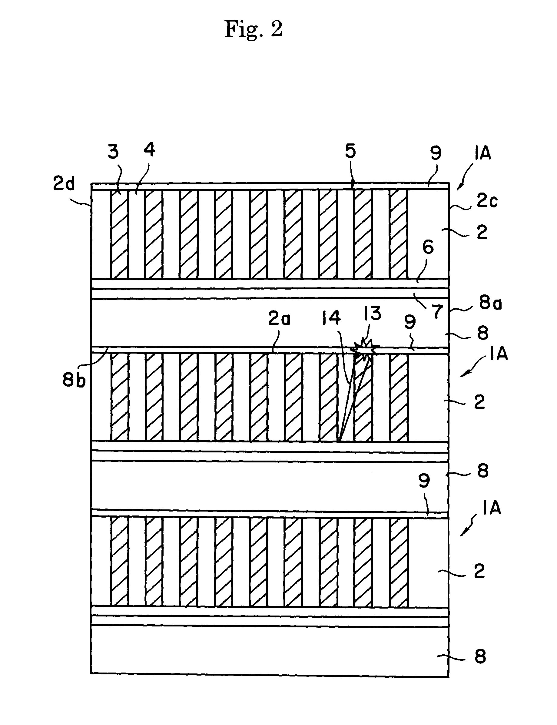
As the inventor has tried to produce the device, however, micro cracks were observed in the region of the optical waveguide of the wavelength conversion substrate.
That is, due to piezoelectric effect during the polishing, abnormal discharge is generated between the upper face of the wavelength conversion substrate of one device and the lower face of the supporting body of the adjacent device on the upper side in the stack.

Method used


Image

  • Wavelength conversion devices and a method of producing the same
  • Wavelength conversion devices and a method of producing the same
  • Wavelength conversion devices and a method of producing the same

Examples


example 1

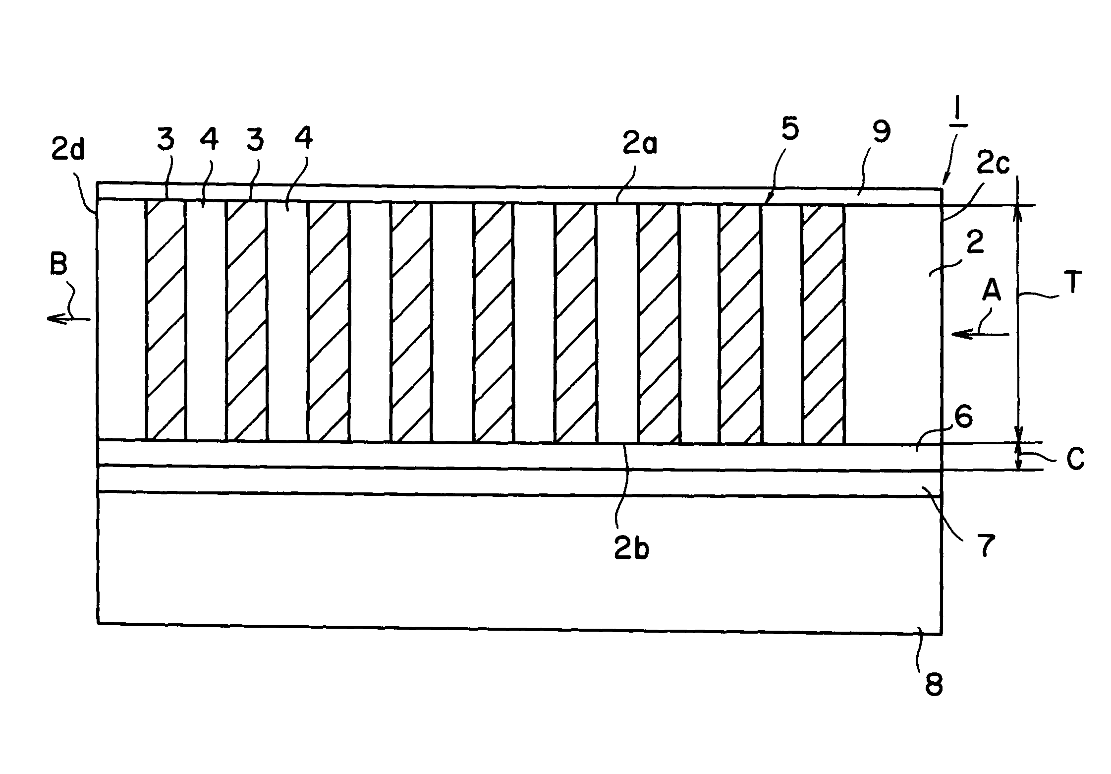
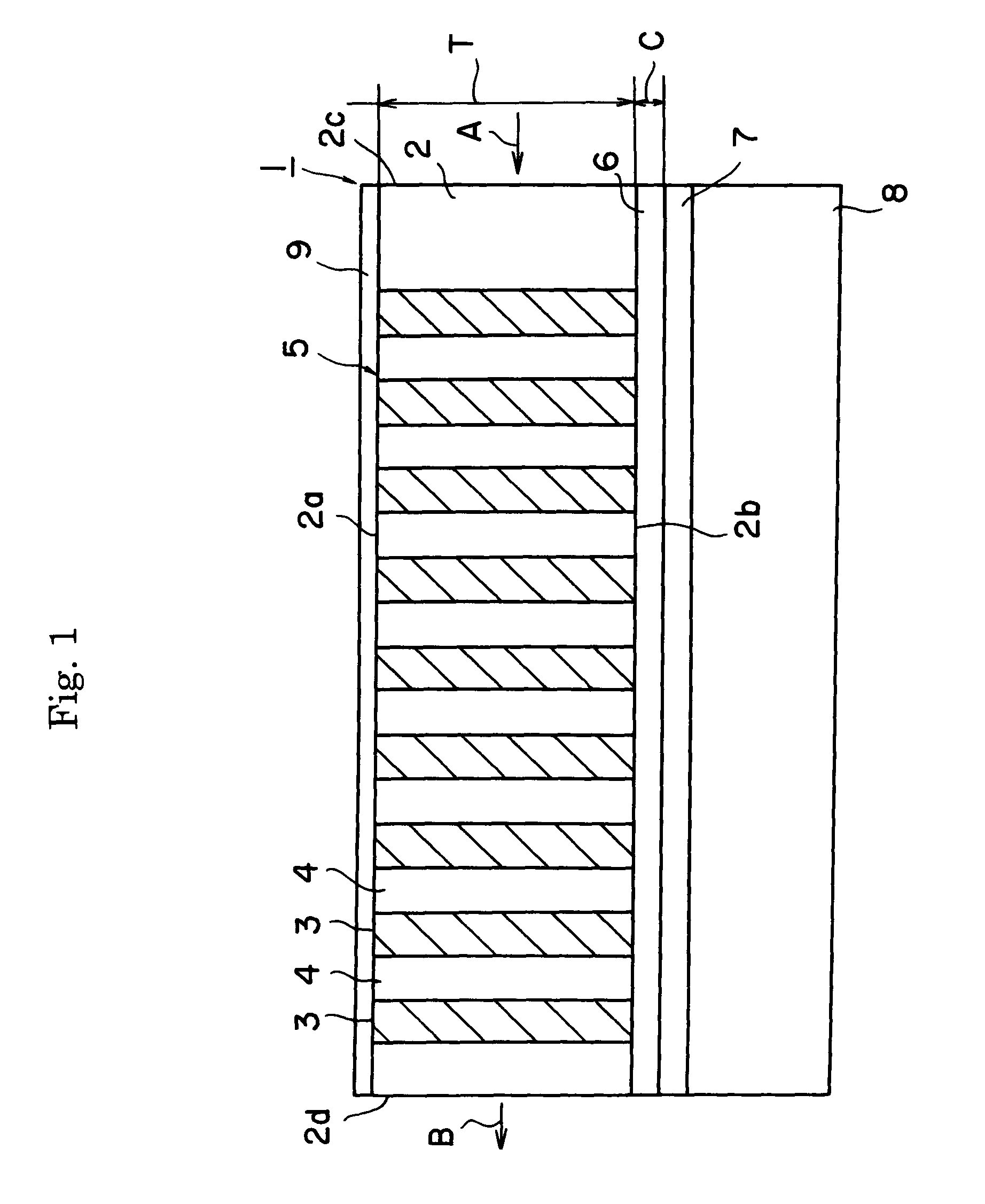
[0065]The second harmonic wave oscillating device illustrated in FIG. 1 was produced.

[0066]Specifically, a comb-shaped periodic electrode with a period of 7.0 μm was formed on an MgO 5% doped lithium niobate Z substrate of 0.5 mm thick by photolithography. The substrate has a volume resistivity of 5×10¹³ Ω·cm. An electrode membrane was formed over the entire surface of the back face of the substrate. A pulse voltage was then applied on the electrodes to form the periodic domain polarization inversion structure 5. An SiO2 under clad (buffer layer) 6 of a thickness of 0.6 μm was formed thereon by sputtering.

[0067]An adhesive was applied on a Z-cut low resistance lithium niobate substrate 8 of a thickness of 0.5 mm, which was then adhered to the above MgO-doped lithium niobate substrate. The substrate 8 had a volume resistivity of 5×10¹⁰ Ω·cm. The thickness of the adhesive was 0.4 μm. The surface of the MgO-doped lithium niobate substrate was ground and polished to a thickness of 45 μm...

example 2

[0070]The second harmonic wave oscillating device 1 was produced according to the same procedure as the Example 1, and its end face was polished. However, the material of the supporting body 8 was a low resistance lithium niobate single crystal having a volume resistivity of 4×10¹¹ Ω·cm.

[0071]Nd-YAG laser was used in the optical waveguide to measure the optical characteristics of the chip. That is, the oscillation power of the laser was adjusted at 2 W to provide a fundamental light, which was incident into the slab optical waveguide through a lens. The fundamental light was scanned over a width of 3 mm and the distribution of the resulting SHG output was measured. It was thus proved that an SHG output power of 10 mW or more was observed over the whole scanned region.

example 3

[0075]The second harmonic wave oscillating device 11 illustrated in FIG. 3 was produced.

[0076]Specifically, a comb-shaped periodic electrode with a period of 7.0 μm was formed on an MgO 5% doped lithium niobate Z substrate of 0.5 mm thick by photolithography. The substrate has a volume resistivity of 5×10¹³ Ω·cm. An electrode membrane was formed over the entire surface of the back face of the substrate. A pulse voltage was then applied on the electrodes to form a periodic domain polarization inversion structure 5. An SiO2 under clad (buffer layer) 6 of a thickness of 0.6 μm was formed thereon by sputtering.

[0077]An adhesive was applied on a lithium niobate substrate 8 of a thickness of 0.5 mm, which was then adhered to the above MgO-doped lithium niobate substrate. The substrate 8 had a volume resistivity of 1×10¹⁴ Ω·cm. The thickness of the adhesive was 0.4 μm. The surface of the MgO-doped lithium niobate substrate was ground and polished to a thickness of 45 μm. An optical wavegui...


PUM

PropertyMeasurementUnit
thicknessaaaaaaaaaa
thicknessaaaaaaaaaa
thicknessaaaaaaaaaa

Abstract

A wavelength conversion device has a supporting body, a wavelength conversion substrate, a lower side buffer layer provided on the side of a bottom face of the substrate, a upper side buffer layer provided on the side of a upper face of the substrate, and an adhesive layer adhering the supporting body 8 and the lower side buffer layer. The wavelength conversion substrate is made of a Z-plate of a ferroelectric single crystal and a periodic polarization inversion structure formed therein. The supporting body has a volume resistivity lower than that of the ferroelectric single crystal of the wavelength conversion substrate.

Description

[0001]This application claims the benefit of Japanese Patent Application No. P2009-51527 filed on Mar. 5, 2009, the entirety of which is incorporated by reference.BACKGROUND OF THE INVENTION[0002]1. Technical Field of the Invention[0003]The present invention relates to a wavelength conversion device and a method of producing the same.[0004]2. Related Art[0005]Non-linear optical crystals, such as lithium niobate and lithium tantalate single crystals, have a high secondary non-linear optical constant. A periodic polarization inversion configuration can be formed in the crystal to produce a Quasi-Phase-Matched (QPM) Secondary-Harmonic-Generation (SHG) device. Further, an optical waveguide may be formed in the periodic polarization inversion configuration to produce a high efficient SHG device, leading to a wide variety of applications in optical communication, medical, photochemical and various optical measurement fields.[0006]According to Japanese patent publication No. 2005-55528A fi...

Claims


Application Information

Patent Timeline
Patent Type & Authority Patents(United States)
IPC IPC(8): G02F1/355G02F1/35G02F2/02
CPCG02F1/3558G02F1/3775Y10T156/10
Inventor YOSHINO, TAKASHI
Owner NGK INSULATORS LTD
Learn More