Optical waveguide devices and harmonic wave generating devices
a technology of harmonic wave generation and optical waveguide, which is applied in the direction of optical waveguide light guide, optical element, instrument, etc., can solve the problems of increasing propagation loss, reduce propagation loss, reduce propagation loss, and prevent the reduction of propagation efficiency
- Summary
- Abstract
- Description
- Claims
- Application Information
AI Technical Summary
Benefits of technology
Problems solved by technology
Method used
Image
Examples
example 1
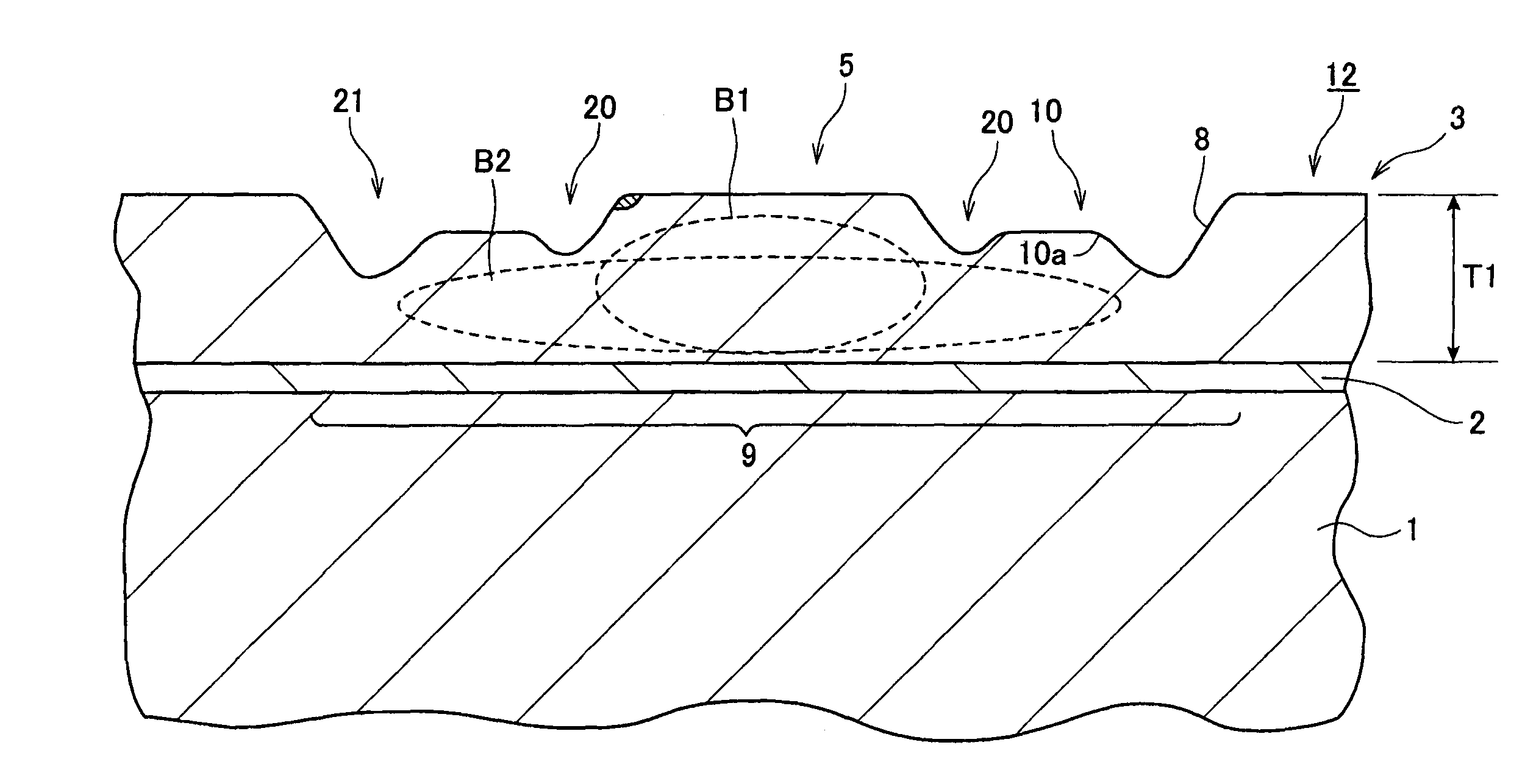
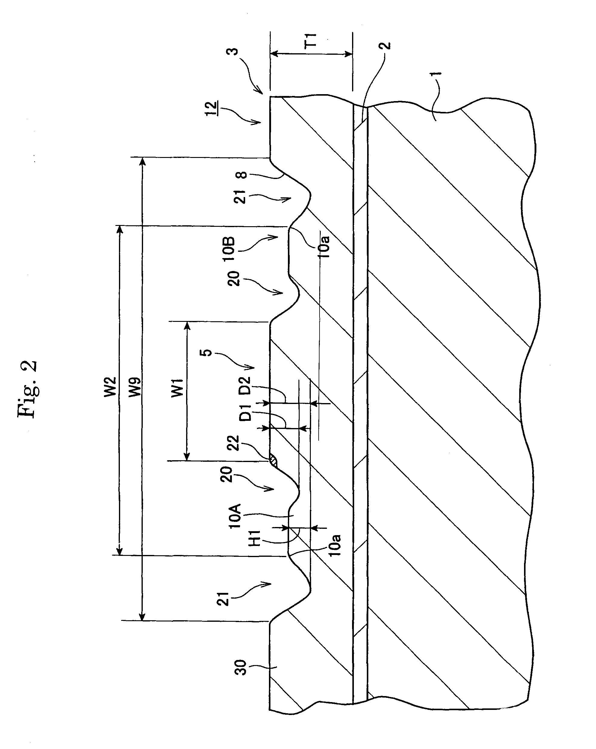
[0084]The device shown in FIG. 2 was produced.
[0085]Specifically, a periodic domain inversion structure of a period of 17.6 μm was formed in an MgO-doped lithium niobate substrate with a thickness of 500 μm, which was then adhered onto a non-doped lithium niobate substrate 1 having a thickness of 1 mm. Then, the exposed surface of the MgO-doped lithium niobate substrate was processed by grinding and polishing to a thickness of 5.0 μm to form the ferroelectric layer 3. Then, the ridge portion, protuberances 10A, 10B, inner grooves 20 and outer grooves 21 were formed by laser ablation. The shape of a processing mask for the laser ablation was changed to adjust the respective dimensions. Further, it was produced a device having a length of 45 mm and the both end faces were polished.
[0086]Besides, the cross section of the device was observed and the depth, width and thickness were measured by means of a critical dimension microscope.
[0087]It was measured the propagation loss of the opti...
example 2
[0091]The devices were produced according to the same procedure as the Example 1 and the propagation losses were measured. However, the thickness T1 of the ferroelectric layer 3 was made 4.0 μm. The other dimensions were changed as shown in the following table 2. The results were shown in table 2.
[0092]
TABLE 2T1W1W2D1D2Propagation loss(μm)(μm)(μm)(μm)(μm)(dB / cm)E-14.05.517.02.03.02.5E-24.06.517.02.03.01.0E-34.06.617.02.03.00.3E-44.07.017.02.03.00.3E-54.08.517.02.03.00.4E-64.09.017.02.03.01.3E-74.06.67.02.03.01.2E-84.06.68.02.03.01.0E-94.06.68.62.03.00.4E-104.06.610.02.03.00.4E-114.06.620.02.03.00.4E-124.06.621.02.03.01.0E-134.06.617.01.03.03.0E-144.06.617.01.753.02.0E-154.06.617.02.53.00.4E-164.06.617.02.93.00.4E-174.06.617.03.03.01.8E-184.06.617.02.02.21.2E-194.06.617.02.02.50.5E-204.06.617.02.03.50.4E-214.06.617.02.04.02.0
[0093]As can be seen from table 2, it was observed tendency similar to that shown in the Example 1.
example 3
[0094]The devices were produced according to the same procedure as the Example 1 and the propagation losses were measured. However, the thickness T1 of the ferroelectric layer 3 was made 7.0 μm. The other dimensions were changed as shown in the following table 3. The results were shown in table 3.
[0095]
TABLE 3PropagationT1W1W2D1D2loss(μm)(μm)(μm)(μm)(μm)(dB / cm)F-17.05.517.02.03.01.9F-27.06.517.02.03.00.8F-37.06.617.02.03.00.3F-47.07.017.02.03.00.3F-57.08.517.02.03.00.5F-67.09.017.02.03.01.2F-77.06.67.02.03.00.8F-87.06.68.02.03.00.8F-97.06.68.62.03.00.4F-107.06.610.02.03.00.4F-117.06.620.02.03.00.4F-127.06.621.02.03.01.0F-137.06.617.01.03.02.0F-147.06.617.01.753.01.3F-157.06.617.02.53.00.4F-167.06.617.02.93.00.5F-177.06.617.03.03.01.5F-187.06.617.02.02.21.0F-197.06.617.02.02.50.5F-207.06.617.02.03.50.3F-217.06.617.02.04.01.2
[0096]As can be seen from table 3, it was observed tendency similar to that shown in the Example 1.
PUM
| Property | Measurement | Unit |
|---|---|---|
| thickness | aaaaa | aaaaa |
| thickness | aaaaa | aaaaa |
| width W1 | aaaaa | aaaaa |
Abstract
Description
Claims
Application Information


