Semiconductor device and method for fabricating the same

a semiconductor device and a technology for fabricating the same, applied in the direction of digital storage, radio frequency controlled devices, instruments, etc., can solve the problems of reducing the process margin required for securing the contact area of the plug, the separation distance between the lower electrodes gets closer, and the drawback as mentioned above still exists in the conventional fabrication of semiconductor devices, so as to prevent a short of the lower electrodes, widen the effective capacitor area, and provide enough capacitance

Inactive Publication Date: 2008-03-04
SK HYNIX INC
View PDF13 Cites 7 Cited by
  • Summary
  • Abstract
  • Description
  • Claims
  • Application Information

AI Technical Summary

Benefits of technology

[0055]A semi-conductor device is disclosed that is capable of preventing a short of lower electrodes caused by a leaning or lifting phenomenon during processes for forming the lower electrodes and while still providing enough capacitance by widening an effective capacitor area. A method for fabricating the same is also disclosed.

Problems solved by technology

However, as the semiconductor device is highly integrated, a drawback such as a reduced process margin required for securing a contact area for a plug still exists.
Such drawback as mentioned above still remains in the semiconductor devices conventionally fabricated.
However, a problem with the method mentioned above still exists as the photo-resist pattern becomes extremely fine, and therefore, the separation distance between the lower electrodes gets closer.
Therefore, a bump such as a meta-stable poly silicon (MPS) used for increasing the capacitance can not be formed due to a short between bumps formed at the bottom plane of the lower electrode.
Furthermore, a dielectric layer and the lower electrode can not be formed due to the short between the bumps.
Such tapering etch profile causes a decrease in the effective capacitance.
The other hand, an excessive etching process along the major axis may be carried out to obtain a vertical etch profile.
Furthermore, a thickness of the deposited lower electrode is decreased due to a narrow critical dimension and thereby, increasing a possibility of the lower electrode being eventually broken.
Consequently, an effective capacitor area is reduced and it becomes difficult to secure the required capacitance.
Furthermore, a possibility that an electrical short is generated by a bridging phenomenon is substantially increased.

Method used


Image

  • Semiconductor device and method for fabricating the same
  • Semiconductor device and method for fabricating the same
  • Semiconductor device and method for fabricating the same

Examples


second embodiment

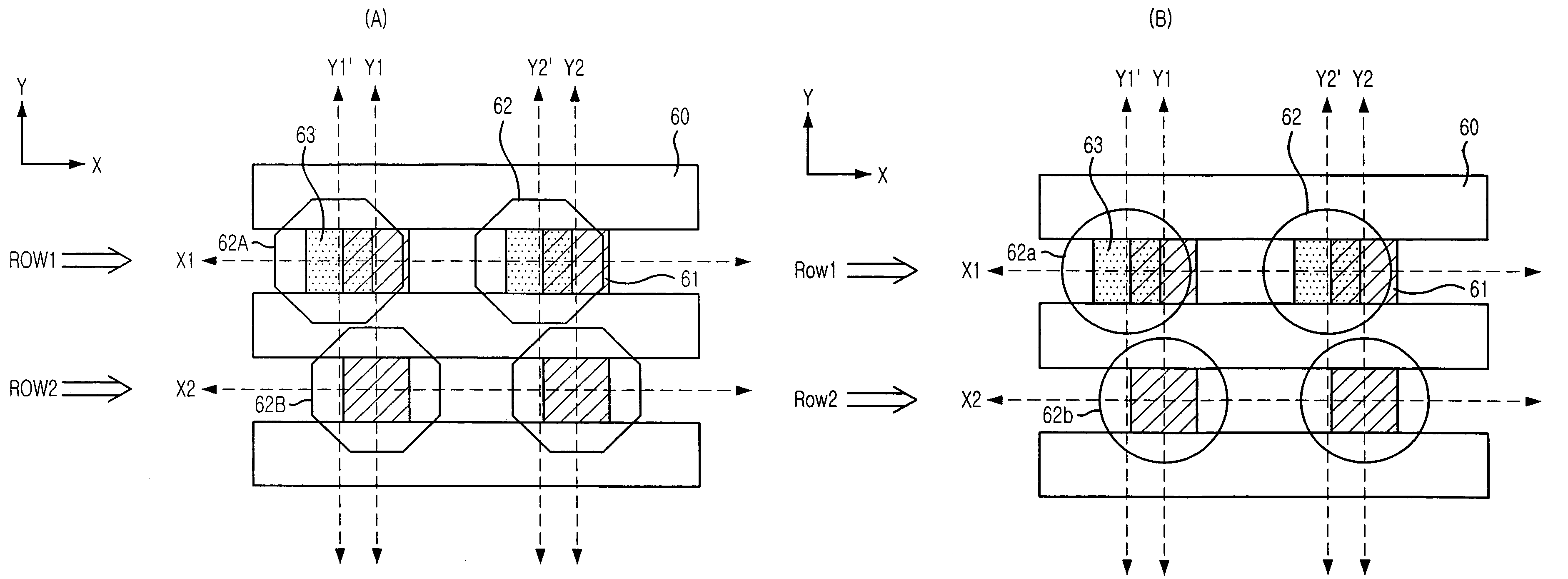
[0097]However, a plurality of contact pads 63 are used to connect the lower electrode 62 with the capacitor plug 61 electrically. To form the contact pad, an extra process is required. However, if the contact pad 63 is applied to the semiconductor device, a contact area of the contact pad 63 is increased. However, the area that the lower electrodes 62 face each other in opposite direction are minimized or even become zero. Herein, the lower electrodes 62, for example, the paired lower electrodes 62A and 62B are located at both sides of the bit line 60.

[0098]As shown in FIG. 9, only along the X virtual axis indicated with a reference mark ‘ROW1’ the contact pads 63 are formed. Also, the midpoint of the contact pad 63 is located at the X virtual axis X1 and the Y virtual axis Y1′. In short, in view of the Y virtual axis, the contact pad 63 is shifted from the Y virtual axis Y1 to the Y virtual axis Y1″. Above-described structural feature is applied to whole layout of the contact pads...

first embodiment

[0099]In addition, as described in the first embodiment, the lower electrodes 62 are formed in the zigzag distribution and thereby, decreasing the area that the paired lower electrodes face each other.

[0100]Consequently, the lifting phenomenon of the lower electrode 62 and the electrical short between the lower electrodes 62 can be considerably reduced or prevented. Also, the pattern collapse phenomenon is prevented by the octagonal or circular shape of the upper plane of the lower electrode 62 and thereby, increasing the capacitance of the capacitor.

[0101]In addition, a contact resistance is also decreased by widening an area of which the contact pad is applied to make the capacitor plug 61 be in contact with the lower electrode 62.

[0102]In FIGS. 10 and 11, the contact pads 63 are formed along all X virtual axis.

[0103]In FIG. 12, the contact pads are formed only along the X virtual axis corresponding to a line indicated with the reference mark ‘ROW2’.

[0104]Referring to FIG. 12, the...


PUM


Abstract

Semiconductor devices and methods of manufacture thereof are disclosed that are capable of preventing a short of lower electrodes caused by a leaning or lifting phenomenon while forming the lower electrodes and securing enough capacitance of a capacitor by widening an effective capacitor area. The inventive semiconductor device includes: a plurality of capacitor plugs disposed in an orderly separation distance; and a plurality of lower electrodes used for a capacitor and disposed in an orderly separation distance to be respectively connected with the capacitor plugs.

Description

TECHNICAL FIELD[0001]A semiconductor memory device is disclosed that includes a lower electrode for a capacitor. A method for fabricating the same is also disclosed.DESCRIPTION OF RELATED ART[0002]Recently, a variety of technologies for improving charge storage capacity has been developed as the size of semiconductor devices is reduced. As a preferable choice, the capacitor has been formed as a three-dimensional (3D) structure. For example, a concave capacitor is a representative capacitor having the 3D structure.[0003]FIGS. 1A to 1C are cross-sectional views showing a conventional method for fabricating a semiconductor device that includes a lower electrode.[0004]As shown in FIG. 1A, a first insulation layer 11 that is an oxide based layer is formed over a semiconductor substrate 11. A first plug 12 is formed to be in contact with the semiconductor substrate 10 by penetrating the first insulation layer 11. The first plug gets to be in contact with an impurity diffusion area such as...

Claims


Application Information

Patent Timeline
Patent Type & Authority Patents(United States)
IPC IPC(8): H01L27/148H01L29/768H01L21/8242G11C8/02H01L21/82H01L27/02H01L27/10H01L27/108
CPCH01L27/10855H01L27/0207H01L27/10814H10B12/315H10B12/0335
Inventor KIM, DONG-SAUKLEE, HO-SEOKPARK, BYUNG-JUNKWON, IL-YOUNGLEE, JONG-MINKIM, HYEONG-SOOKIM, JIN-WOONGCHOI, HYUNG-BOKSHIN, DONG-WOO
Owner SK HYNIX INC
Why Eureka
Try Eureka