

Method for forming capacitor of semiconductor device
a technology of semiconductor devices and capacitors, which is applied in the direction of capacitors, semiconductor devices, electrical equipment, etc., can solve the problems of difficult to increase the capacitance of the capacitor, the capacitor cannot be highly integrated to match the size of the cell, and the electric charge storage in the capacitor is difficult to achiev
- Summary
- Abstract
- Description
- Claims
- Application Information
AI Technical Summary
Benefits of technology
Problems solved by technology
Method used
Image

Examples
Embodiment Construction
[0026] Hereinafter, a preferred embodiment of the present invention will be described with reference to the accompanying drawings. In the following description and drawings, the same reference numerals are used to designate the same or similar components, and so repetition of the description on the same or similar components will be omitted.
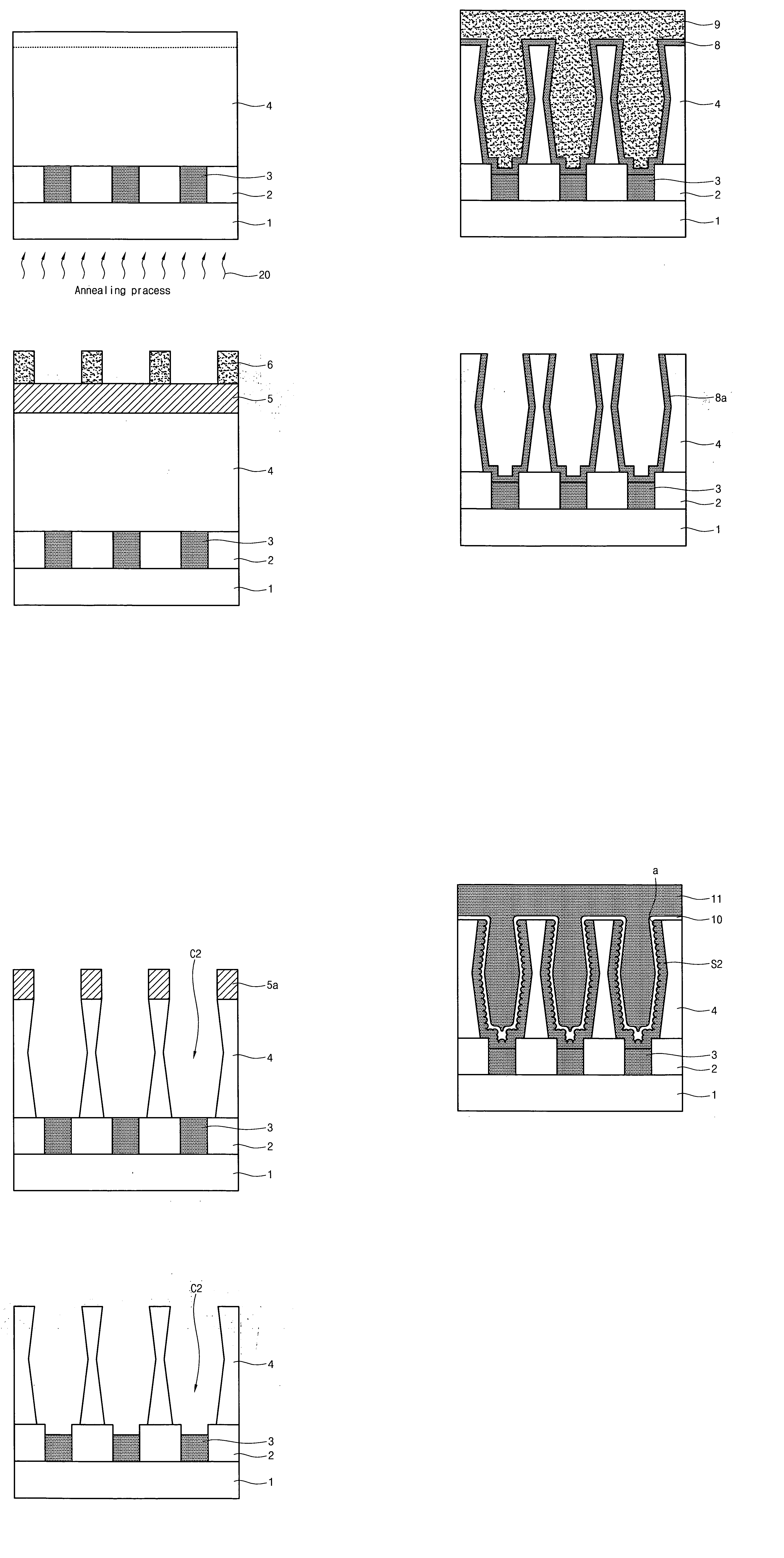
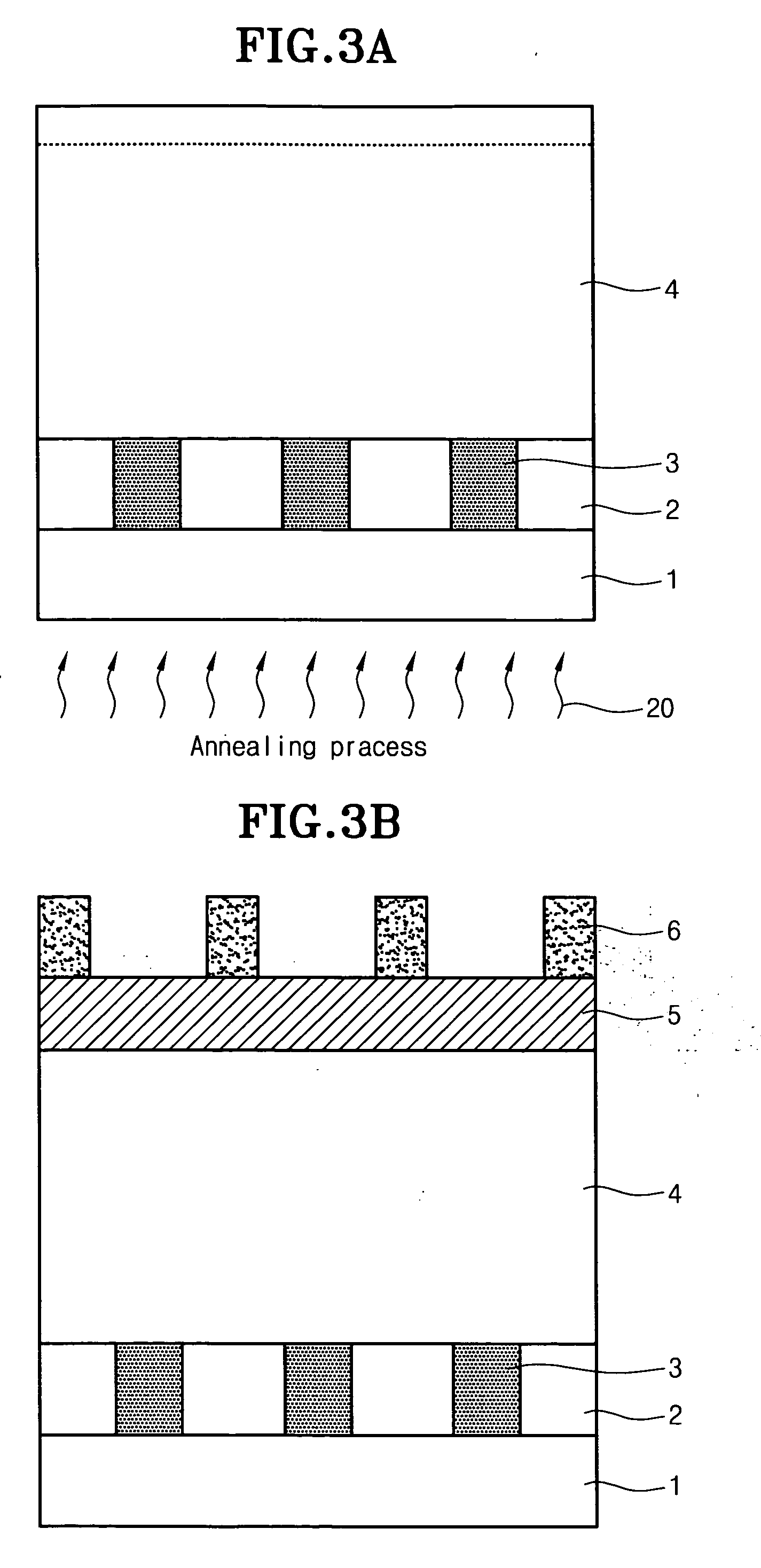
[0027] Hereinafter, a method for forming a capacitor of a semiconductor device according to one embodiment of the present invention will be explained with reference to FIGS. 3a to 3g.
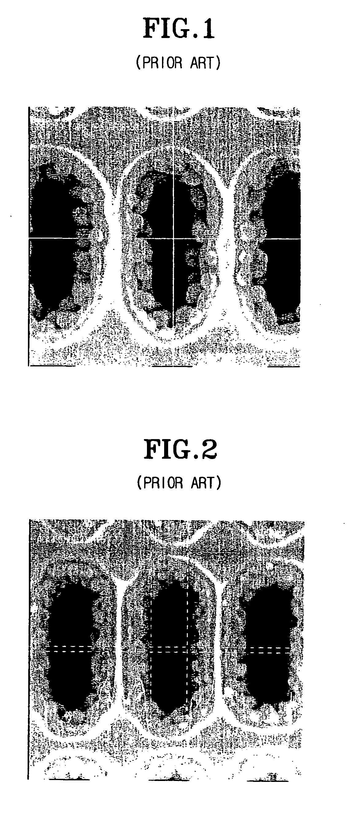
[0028]FIGS. 3a to 3g are views showing a method for forming a capacitor of a semiconductor device according to one embodiment of the present invention.
[0029]FIGS. 3a to 3g are views showing a method for forming a capacitor of a semiconductor device according to another embodiment of the present invention.
[0030] As shown in FIG. 3a, the method for forming the capacitor of the semiconductor device according to another embodiment of the present invention include a s...
PUM
 Abstract
Description
Claims
Application Information