

Nonvolatile semiconductor memory devices and the fabrication process of them
a semiconductor memory and nonvolatile technology, applied in semiconductor devices, solid-state devices, instruments, etc., can solve the problems of inconvenient batch forming, short between memory cells, and conflicting conventional methods, so as to ensure the capacitance, adequate capacitance, and the effect of enlargement of the surface area
- Summary
- Abstract
- Description
- Claims
- Application Information
AI Technical Summary
Benefits of technology
Problems solved by technology
Method used
Image

Examples
first embodiment
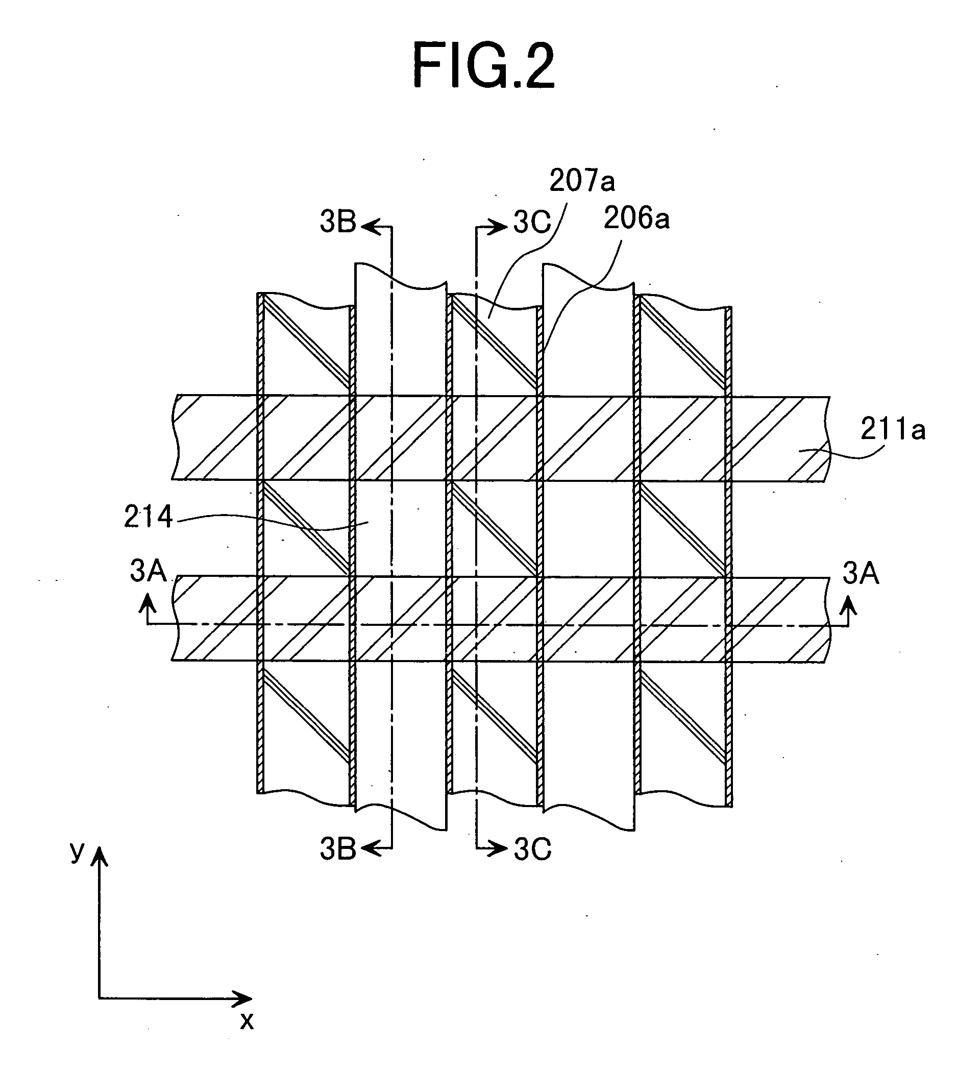
[0084]FIG. 1 is a diagram showing an equivalent circuit of a memory cell according to the present invention. FIG. 2 is a plan view showing an example of a semiconductor integrated circuit device which is a first embodiment according to the present invention. Some components included in the device are omitted in FIG. 2 in order to facilitate understanding of an arrangement of main wirings. FIGS. 3A to 3C are sectional views taken along the lines 3A-3A, 3B-3B, and 3C-3C in FIG. 2.
[Basic Structure of Memory Cell in First Embodiment]
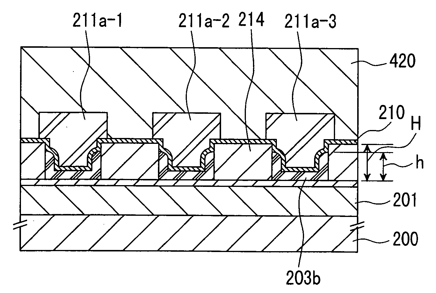
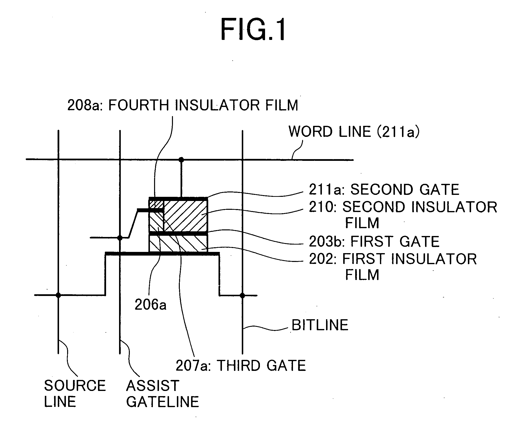
[0085] A memory cell according to the first embodiment will hereinafter be described briefly with reference to FIG. 1. The memory cell of the present embodiment is a cell of a so-called flash memory, which has, like known memory cells, a word line 211a, a bit line, a source line, a first gate 203b which is a floating gate, a second gate 211a which will serve as a control gate, and a third gate 207a. The third gate is a so-called erase gate.
[0086] Although...
second embodiment
[0134] In the first embodiment, after exposing the fourth insulating layers 208a as shown in FIG. 7C, the fifth insulating layers 214 are selectively etched by using the resist pattern as the mask. In the selective etching process, it is possible to etch also the fourth insulating layers 208a to a certain extent with a reduced ratio of the selection. If portions of the fourth insulating layers 208a are etched, a height of side walls of each of the fifth insulating layers 214 becomes greater than those of the third gates 207a and the fourth insulating layers 208a as it is apparent when viewed from the spaces formed through the first gate oxide film 202 on the silicon substrate.
[0135] In the present embodiment, process steps shown in FIGS. 6A to 7C are performed in the same manner as in the first embodiment, and the fourth insulating layers 208a are etched to a somewhat large extent as mentioned above. After that, in the same manner as in the first embodiment, silicon oxide films 206...
third embodiment
[0145] In the first and second embodiments, the fifth insulating layer 214 is deposited followed by the exposition of the fourth insulating layers 208a and then the fifth insulating layer 214 is processed to form the spaces 230 on the first gate oxide film 202 over the silicon substrate.
[0146] In turn, in the third embodiment, the fifth insulating layer 214 is patterned in a state where the fourth insulating layers 208a are covered perfectly with the fifth insulating layer 214 by a dry etching technique using the resist pattern as a mask. In this case, even if the etching is performed under the condition of selectively etching the fifth insulating layer 214, a height H1 of the insulating layers 214 is originally greater than a height h1 of the fourth insulating layers 208a.
[0147] More specifically, in the present embodiment, process steps until FIG. 7B are the same as those of the first embodiment. Sectional views of the process step taken along the lines 21A-21A, 21B-21B, and 21C...
PUM
 Abstract
Description
Claims
Application Information