Memory device and method for operating a memory device

a memory device and memory technology, applied in the field of memory device and memory device operation, can solve problems such as affecting the threshold voltage, and achieve the effects of improving the reliability of programming operation of memory devices, improving programming of memory devices, and uniform programming operation

Inactive Publication Date: 2008-03-11
POLARIS INNOVATIONS LTD
View PDF5 Cites 2 Cited by
  • Summary
  • Abstract
  • Description
  • Claims
  • Application Information

AI Technical Summary

Benefits of technology

[0012]In one aspect, the present invention improves programming of memory devices that include a plurality of equally-sized memory areas. In particular, one embodiment of the invention obtains a uniform performance of programming operation that is less dependent on the position of the memory cell within the memory array. Furthermore, in another aspect, the invention compensates varying magnitudes of the threshold voltage of the memory cells comprised in the memory device and to improve reliability of programming operation of a memory device.

Problems solved by technology

Furthermore, other intrinsic and systematic design related effects also may influence the threshold voltage.

Method used


Image

  • Memory device and method for operating a memory device
  • Memory device and method for operating a memory device
  • Memory device and method for operating a memory device

Examples


Embodiment Construction

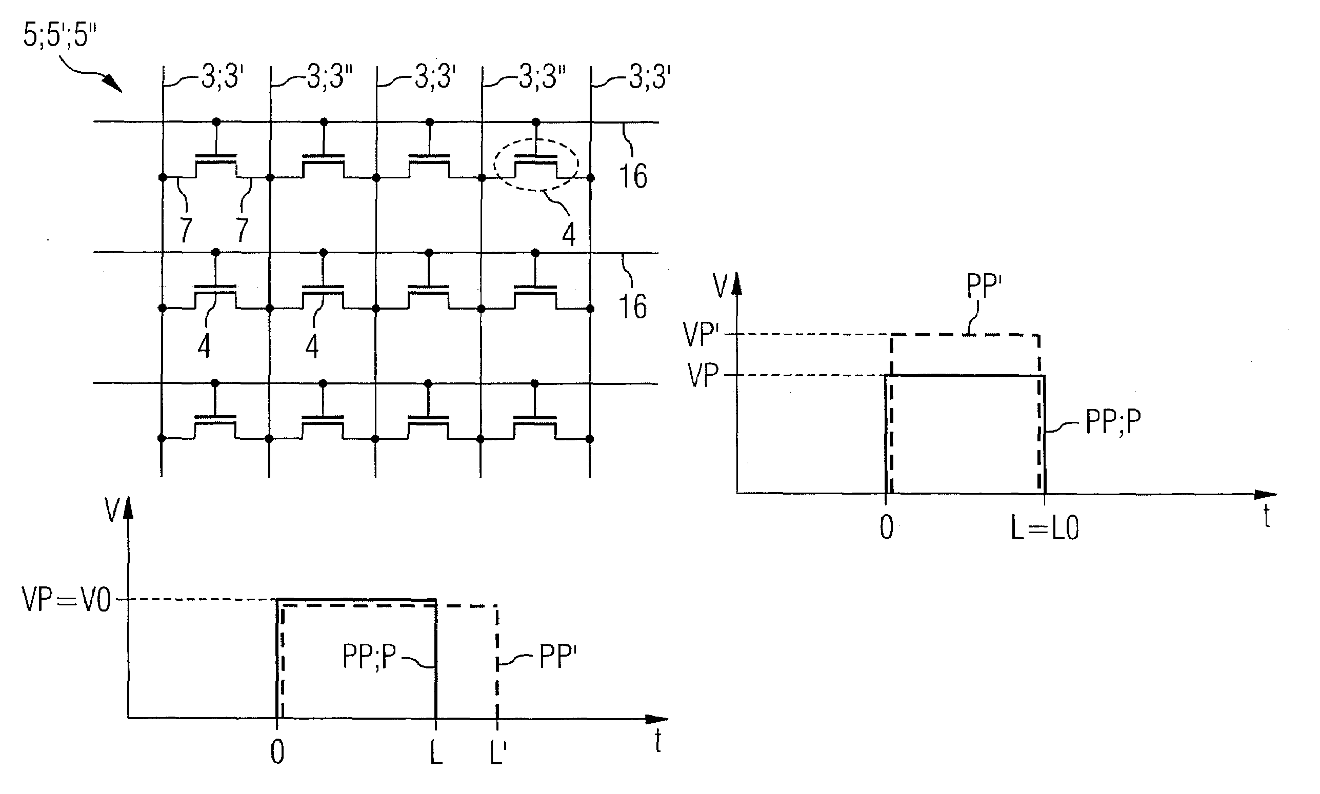
[0073]FIG. 1 illustrates a top view of a memory device 1 according to embodiments of the present invention. The memory device 1 comprises a memory array 2, which comprises a plurality of non-volatile memory cells. The memory cells are connected to conductive lines 3 which, for instance, may be bitlines. The memory array 2 preferably is a flash memory array comprising NROM memory cells or another kind of non-volatile memory cells. In case of a flash memory, the memory array 2 may be subdivided into plural sectors 10 comprising memory cells that can only be erased simultaneously within a particular sector. Accordingly, any memory cell within a sector is erased simultaneously with all other memory cells of the same sector 10.

[0074]Irrespective of whether the memory array 2 is subdivided in sectors 10 or is not, the memory array 2 in any case comprises a plurality of memory areas 5 that each are equally-sized and each comprise the same number of conductive lines 3 and the same number of...


PUM


Abstract

A memory device (1) includes a memory array (2). The memory array (2) has at least one memory area (5) that includes a plurality of conductive lines (3) and a plurality of memory cells (4) connected to the conductive lines (3). The conductive lines (3) are arranged at positions (n) within the memory area (5). The memory cells (4) are erasable and are programmable by application of an electrical programming pulse (P) supplied via a respective conductive line (3). The memory device (1) is constructed such that for programming of a memory cell (4) an electrical programming pulse (P) is applied which has a programming pulse profile (PP) depending on the position (n) of a respective conductive line (3) to which the memory cell (4) is connected.

Description

TECHNICAL FIELD[0001]The present invention relates generally to semiconductor devices and methods and, in a particular embodiment, to a memory device and method for operating a memory device.BACKGROUND[0002]The invention relates to memory devices comprising a memory array having a plurality of non-volatile memory cells, like NROM memory devices (nitride read only memory) or devices comprising floating gate transistor cells, for instance. The invention in particular refers, for instance, to flash memory devices comprising sectors of non-volatile memory cells, all memory cells of a particular sector being erased commonly if an erasing operation is performed in the respective sector of the memory array. The invention further refers to memory devices comprising memory cells that each are capable of storing at least one first bit at a first bit position and at least one second bit at a second bit position different from the first bit position, like twin-flash memory cells and multi-level...

Claims


Application Information

Patent Timeline
Patent Type & Authority Patents(United States)
IPC IPC(8): G11C11/34
CPCG11C16/0475G11C16/0491G11C29/02G11C29/021G11C29/028G11C16/04G11C16/10
Inventor KOEBERNICK, GERTSEIDEL, KONRADAUGUSTIN, UWE
Owner POLARIS INNOVATIONS LTD
Why Eureka
Try Eureka