
Semiconductor memory device

a memory device and semiconductor technology, applied in the direction of digital storage, substation/switching arrangement details, instruments, etc., can solve the problems of increased cost and time to manufacture the semiconductor memory device, and the semiconductor memory device does not have a means, so as to improve the resulting stability of the internal voltage and increase the capacity to supply the internal voltage

Inactive Publication Date: 2008-03-11
SAMSUNG ELECTRONICS CO LTD
View PDF12 Cites 4 Cited by
  • Summary
  • Abstract
  • Description
  • Claims
  • Application Information

AI Technical Summary

Benefits of technology

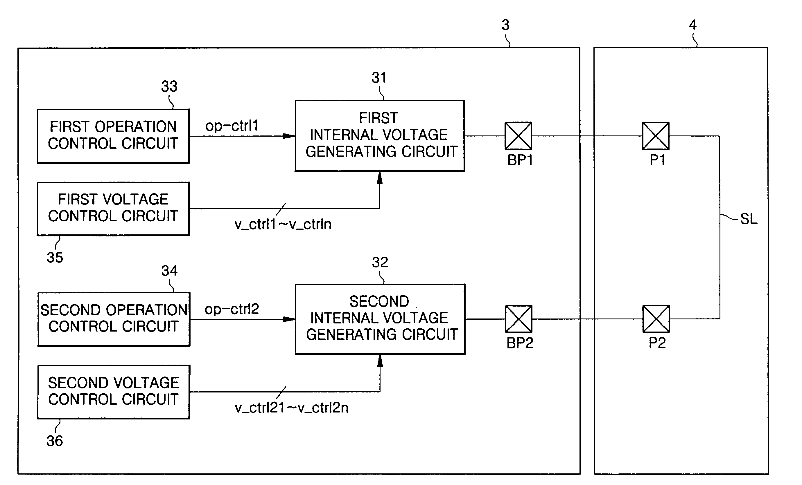
[0014]It is another object of the present invention to provide a semiconductor memory device in which a plurality of internal voltage generating circuits which are connected to each other via a packaging substrate can generate internal voltages having the same level, thereby increasing capability to supply the internal voltage and improving the resulting stability of the internal voltage.

Problems solved by technology

However, the conventional semiconductor memory device does not have a means for selecting the suitable internal voltage generating circuit among certain internal voltage generating circuits and to replace certain internal voltage generating circuits as the selected internal voltage generating circuit in a final, manufactured state of the semiconductor memory device.
Accordingly, there is a problem in that cost and time to manufacture the semiconductor memory device are increased as a result.

Method used


Image

  • Semiconductor memory device
  • Semiconductor memory device
  • Semiconductor memory device

Examples


Embodiment Construction

[0038]The present invention will now be described more fully hereinafter with reference to the accompanying drawings, in which preferred embodiments of the invention are shown. This invention may, however, be embodied in different forms and should not be construed as limited to the embodiments set forth herein. Rather, these embodiments are provided so that this disclosure will be thorough and complete. In the drawings, the thickness of layers and regions are exaggerated for clarity. Like numbers refer to like elements throughout the specification.

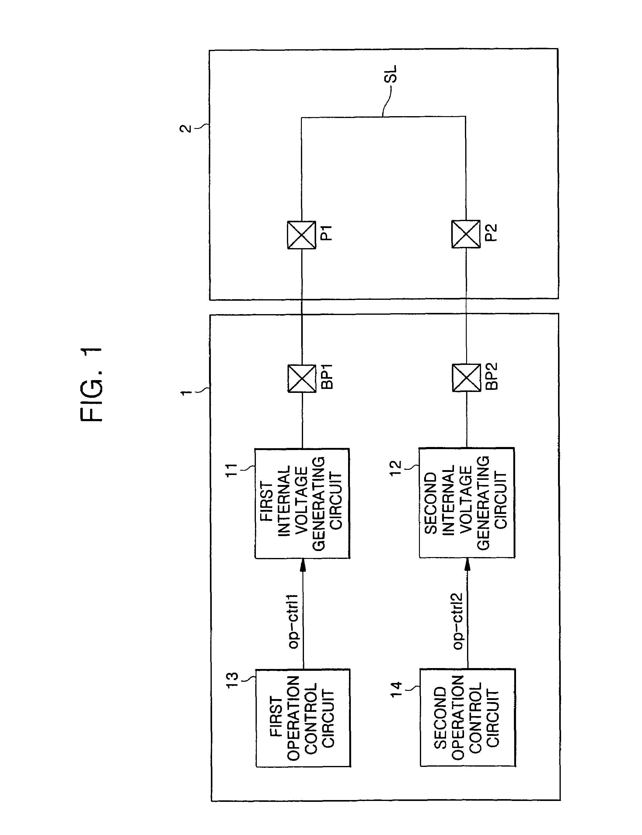
[0039]FIG. 1 is a block diagram illustrating a semiconductor memory device according to an embodiment of the present invention.

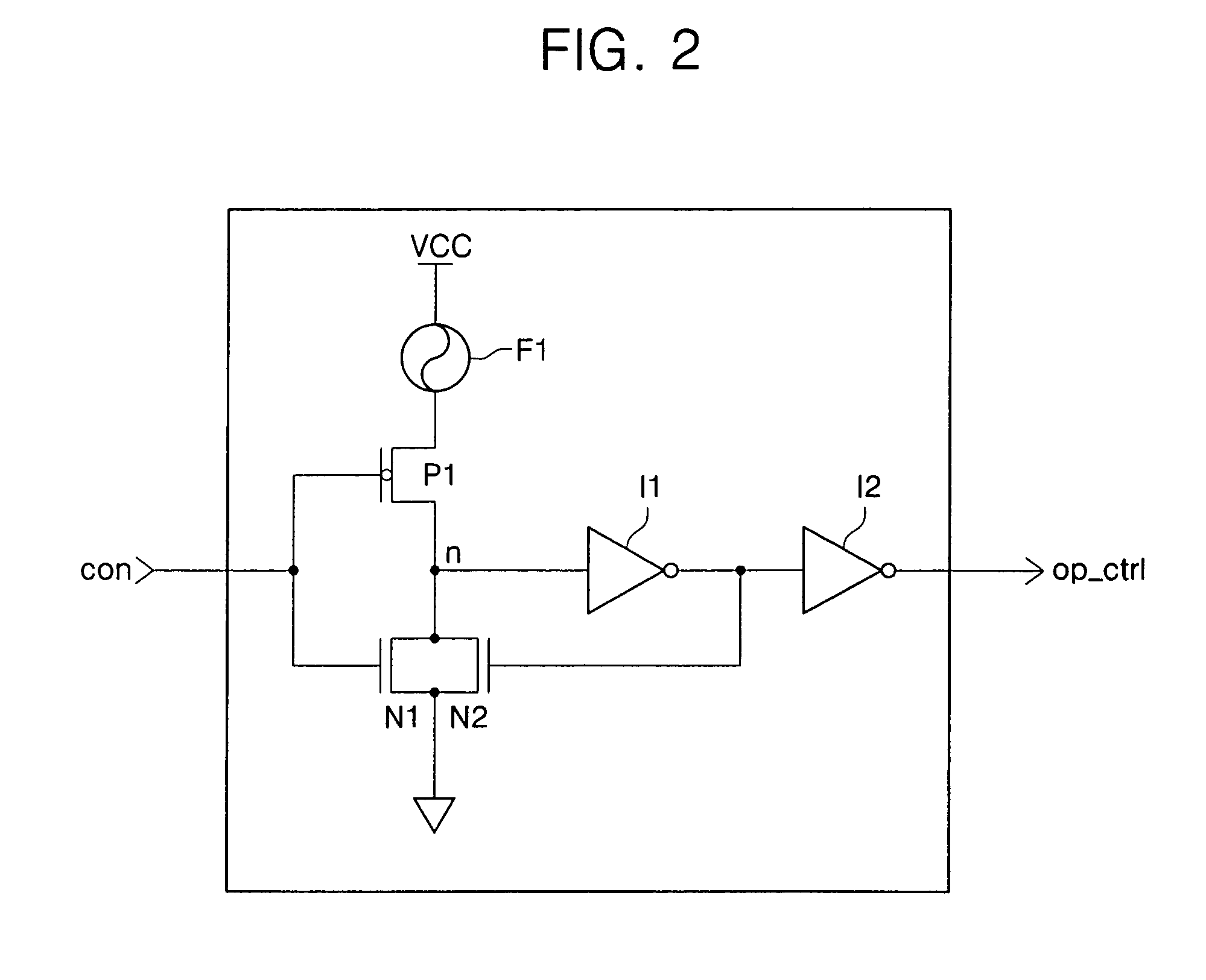
[0040]Referring to FIG. 1, the semiconductor memory device includes a semiconductor chip 1 and a packaging substrate 2. The semiconductor chip 1 includes a first internal voltage generating circuit 11, a second internal voltage generating circuit 12, a first operation control circuit 13, a second operation control ...


PUM


Abstract

A semiconductor memory device includes a semiconductor chip including a first voltage generating circuit that generates a first voltage in response to a first operation control signal, a second voltage generating circuit that generates a second voltage in response to a second operation control signal, a first operation control circuit that generates the first operation control signal, a second operation control circuit that generates the second operation control signal, a first bonding pad connected to an output of the first voltage generating circuit, and a second bonding pad connected to an output of the second voltage generating circuit. A packaging substrate includes a first substrate pad connected to the first bonding pad and a second substrate pad connected to the second bonding pad. The first and second substrate pads are connected to each other through the packaging substrate.

Description

CROSS-REFERENCE TO RELATED APPLICATION[0001]This application claims the benefit of Korean Patent Application No. 2005-61430, filed Jul. 07, 2005, the disclosure of which is hereby incorporated herein by reference in its entirety.BACKGROUND OF THE INVENTION[0002]1. Field of the Invention[0003]The present invention relates to a semiconductor memory device and, more particularly, to a semiconductor memory device which can control respective operations of a plurality of internal voltage generating circuits when the semiconductor device is in a packaged state.[0004]2. Description of the Related Art[0005]Generally, a semiconductor memory device includes a plurality of internal voltage generating circuits which generate internal voltages which are necessary for operation of the semiconductor memory device by using an external power voltage supplied from an external location.[0006]In the case of a dynamic random access memory (DRAM), the semiconductor memory device includes a VPP voltage ge...

Claims


Application Information

Patent Timeline
Patent Type & Authority Patents(United States)
IPC IPC(8): G11C7/00
CPCG11C5/14G11C7/1045G11C11/4074G11C2207/105G11C5/06
Inventor PARK, CHUL-WOO
Owner SAMSUNG ELECTRONICS CO LTD
Learn More