Creation of anisotropic strain in semiconductor quantum well

a quantum well and anisotropic technology, applied in the field of semiconductor electrooptic devices, can solve the problems of difficult to achieve proper anisotropic strain, additional and often expensive complications in the manufacturing process, and the bonding and lifting off procedures

Inactive Publication Date: 2008-03-25
SEC OF THE ARMY UNITED STATES OF AMERICA AS REPRESENTED BY THE
View PDF8 Cites 0 Cited by
  • Summary
  • Abstract
  • Description
  • Claims
  • Application Information

AI Technical Summary

Benefits of technology

[0013]The second crystalline layer (e.g., GaN) can be grown at a temperature of approximately 1000° C. Thus, at room temperature, a thermally induced anisotropic strain can be achieved. Additionally, GaN is chosen for use in forming the second crystalline layer, it can be utilized as an anti-reflection layer, because GaN is transparent. By properly choosing the thickness of the second crystalline layer, a desired anisotropic strain as well as a desired anti-reflection wavelength can be achieved.

Problems solved by technology

One of the problems associated with spatial light modulators, such as that disclosed in U.S. Pat. No. 5,381,260, is that it is difficult to achieve proper anisotropic strain without the removal of the semiconductor substrate upon which the spatial light modulator is formed, or without using another substrate.
Additionally, bonding and lift-off procedures offer additional and often expensive complications to the manufacturing process.

Method used


Image

  • Creation of anisotropic strain in semiconductor quantum well
  • Creation of anisotropic strain in semiconductor quantum well
  • Creation of anisotropic strain in semiconductor quantum well

Examples


Embodiment Construction

[0017]The particular values and configurations discussed in these non-limiting examples can be varied and are cited merely to illustrate embodiments of the present invention and are not intended to limit the scope of the invention.

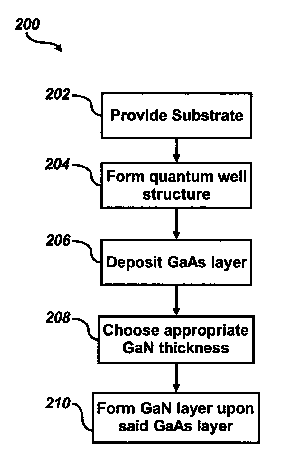
[0018]FIG. 1 illustrates a perspective view 100 of a quantum well structure, which can be implemented in accordance with a preferred embodiment of the present invention. FIG. 1 depicts a substrate 102 upon which an MQW layer 104 (i.e., a quantum well layer) can be formed. A first crystalline layer, such as, for example, a GaAs layer 106, can be deposited upon the MQW layer 104. Thereafter, a second crystalline layer, such as, for example, a GaN layer 108, can be formed upon the GaAs layer 106. Note that in general, the second crystalline layer possesses a crystalline phase, which is different than the crystalline phase of the layer upon which it is deposited.

[0019]It can be appreciated by those skilled in the art that although GaAs and GaN are described he...


PUM


Abstract

Methods and devices for creating an anisotropic strain in a semiconductor quantum well structure to induce anisotropy thereof are disclosed herein. Initially, a substrate is provided, and a quantum well structure formed upon the substrate. A first crystalline layer (e.g., a GaAs layer) having a first crystalline phase can then be deposited upon the quantum well structure. Thereafter, a second crystalline layer (e.g., a GaN layer) having a second crystalline phase and a thickness thereof can be formed upon the first crystalline layer to thereby induce an anisotropic strain in the quantum well structure to produce a quantum well device thereof. Additionally, the second crystalline layer (e.g., GaN) can be formed from a transparent material and utilized as an anti-reflection layer. By properly choosing the thickness of the second crystalline layer (e.g., a GaN layer), a desired anisotropic strain as well as a desired anti-reflection wavelength can be achieved.

Description

STATEMENT OF GOVERNMENT INTEREST[0001]The invention described herein may be manufactured and used by or for the United States Government for Governmental purposes without the payment of any royalties.TECHNICAL FIELD[0002]The present invention generally relates to semiconductor devices. The present invention is also related to semiconductor electro-optic devices. The present invention is additionally related to high contrast light modulators used in real time object and pattern recognition, and to infrared, detection and imaging techniques and devices thereof.BACKGROUND OF THE INVENTION[0003]A variety of electro-optic devices are utilized in scientific, commercial, industrial and consumer applications. Semiconductor multiple quantum well (MQW) modulators represent a type of electro-optic device possessing a broad range of application capabilities. Semiconductor MQW modulators generally operate with incident light normal to the plane of the device. Such devices are well known in the a...

Claims


Application Information

Patent Timeline
Patent Type & Authority Patents(United States)
IPC IPC(8): H01L21/20H01L29/15
CPCB82Y20/00G02F1/01725H01L21/02403H01L21/02507H01L21/0254H01L21/02546H01L29/205G02F2001/0157H01L29/2003H01L33/06G02F1/0157
Inventor WRABACK, MICHAELDUTTA, MITRASHEN, PAUL HONGEN
Owner SEC OF THE ARMY UNITED STATES OF AMERICA AS REPRESENTED BY THE
Why Eureka
Try Eureka