Preparation method of non-rectangular III-V semiconductor quantum well based on bismuth element

A III-V, semiconductor technology, applied in the direction of semiconductor devices, electrical components, circuits, etc., can solve the problems of large strain accumulation, limit the scope of material design and growth, and unfavorable growth of high-quality materials, so as to achieve simple and convenient operation process, The effect of large degrees of freedom

Active Publication Date: 2016-07-06
SHANGHAI INST OF MICROSYSTEM & INFORMATION TECH CHINESE ACAD OF SCI
View PDF3 Cites 1 Cited by
  • Summary
  • Abstract
  • Description
  • Claims
  • Application Information

AI Technical Summary

Problems solved by technology

With the deepening of research, this rectangular quantum structure also brings some restrictions. For example, in addition to the material composition, the variable parameter of the rectangular quantum structure is the width of the potential well and barrier, so the design requirements for some special functions often cannot Satisfied; another example: for the material system using lattice mismatch, the rectangular quantum structure with sudden composition often causes a large strain accumulation, which limits the scope of material design and growth on the one hand, and is not conducive to high quality on the other hand. material growth

Method used


Image

  • Preparation method of non-rectangular III-V semiconductor quantum well based on bismuth element
  • Preparation method of non-rectangular III-V semiconductor quantum well based on bismuth element

Examples


Embodiment 1

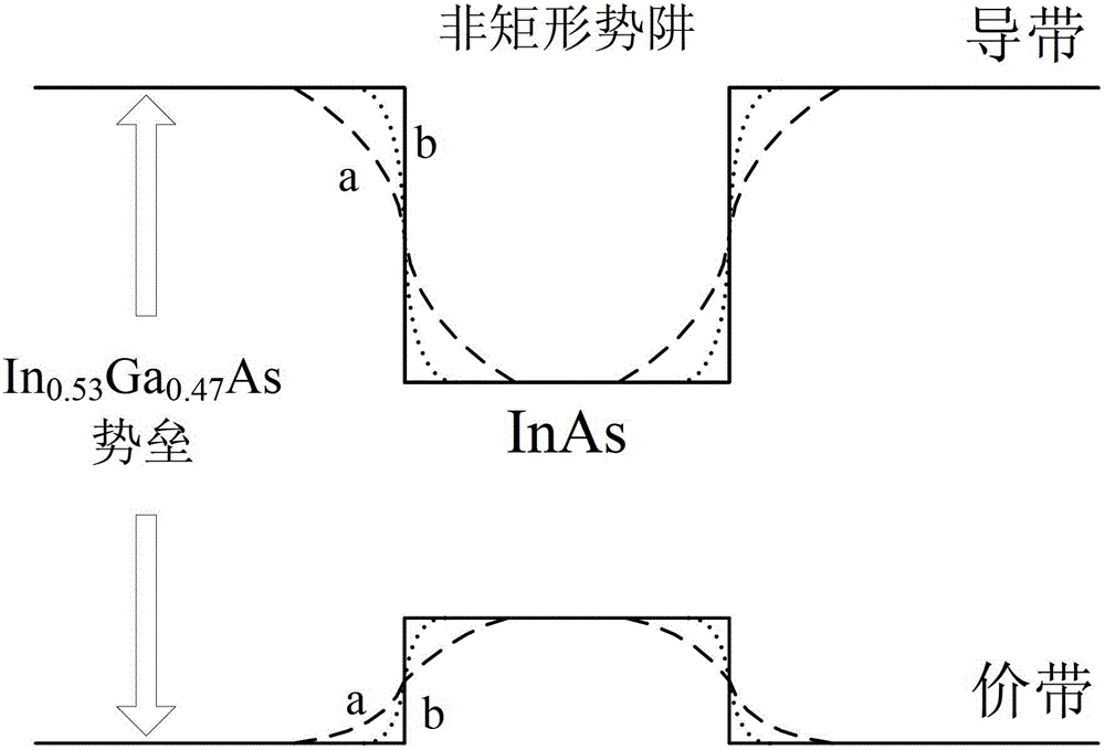
[0018] The following is based on the InP substrate 0.53 Ga 0.47 As / InAs non-rectangular quantum well preparation method is taken as an example to illustrate the preparation method of non-rectangular III-V group semiconductor quantum well based on bismuth:

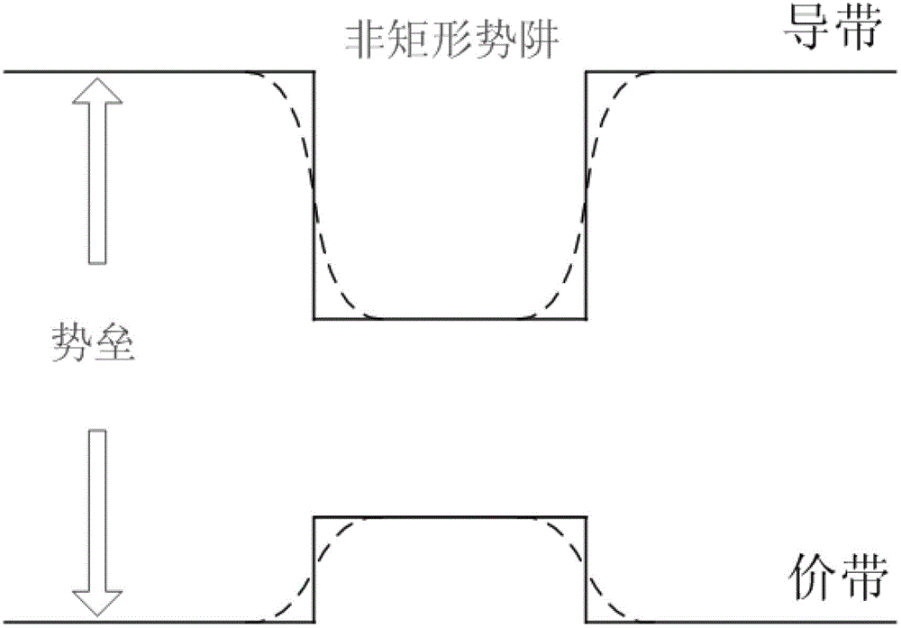
[0019] (1) Need to grow InP on InP substrate 0.53 Ga 0.47 As is the potential barrier, In 0.53 Ga 0.47 As / InAs is a quantum well structure with a non-rectangular potential well;

[0020] (2) The epitaxial growth adopts the conventional molecular beam epitaxy method, Mr. Long In 0.53 Ga 0.47 As barrier, then grow InAs as the bottom of the potential well, and then grow In 0.53 Ga 0.47 As barrier (such as figure 2 As shown by the middle solid line), when the bismuth beam source shutter is opened during the growth of the quantum well, the bismuth element will cause the inter-diffusion of In and Ga at the interface, making the quantum well form a non-rectangular structure (such as figure 2 Shown by dotted line a and dotted line b)....


PUM


Abstract

The invention relates to a preparation method for a bismuth-based non-rectangular group III-V semiconductor quantum well. The preparation method comprises the step of growing a potential well material and a potential barrier material of a group III-V semiconductor quantum well, wherein bismuth is added in the growth processes of both the potential well material and the potential barrier material. According to the preparation method, bismuth beam source shutters are opened simultaneously in the processes of growing the potential well material and the potential barrier material of the quantum well, and a non-rectangular quantum well structure is realized by utilizing the group III element interdiffusion caused by the bismuth. By the method, material components can be controlled effectively; the problem that the conventional growth method is only suitable for growing a rectangular quantum well structure with component mutations is solved; greater freedom is introduced to the design and the implementation of the structure and the functional of quantum; the preparation method disclosed by the invention is suitable for adopting a plurality of material growth means, such as molecular beam epitaxy and atomic layer deposition; and the operation process is simple and convenient.

Description

Technical field [0001] The invention belongs to the field of preparation of semiconductor microstructure materials, and particularly relates to a preparation method of a non-rectangular III-V group semiconductor quantum well based on bismuth. Background technique [0002] With the development of thin film material epitaxy methods and semiconductor physics knowledge, quantum microstructures have been successfully prepared experimentally, which has promoted the rapid development of optoelectronic devices and electronic devices such as semiconductor lasers and semiconductor detectors. These devices have been widely used in different fields, and have played an important role in people's deep understanding and development of various quantum theories. At the same time, they have also promoted molecular beam epitaxy (MBE) and metal organic vapor phase epitaxy (MOCVD). The development of thin-layer epitaxy methods. At present, the quantum structure used is mainly based on heterogeneous ...

Claims


Application Information

Patent Timeline
Patent Type & Authority Patents(China)
IPC IPC(8): H01L33/00H01L33/06H01L33/30
Inventor 王庶民顾溢宋禹忻叶虹
Owner SHANGHAI INST OF MICROSYSTEM & INFORMATION TECH CHINESE ACAD OF SCI
Why Eureka
Try Eureka