

Method for producing terahertz radiation of semiconductor quantum trap negative effective mass device
A technology of terahertz radiation and effective mass, which is applied in the field of semiconductor optoelectronic materials and devices, and can solve the problems of bulky and inconvenient use
Inactive Publication Date: 2006-08-23
SHANGHAI INST OF MICROSYSTEM & INFORMATION TECH CHINESE ACAD OF SCI
View PDF0 Cites 1 Cited by
- Summary
- Abstract
- Description
- Claims
- Application Information
AI Technical Summary
Problems solved by technology
But it is bulky and inconvenient to use
Method used
View moreImage
Smart ImageViewing Examples

Examples
Embodiment 1
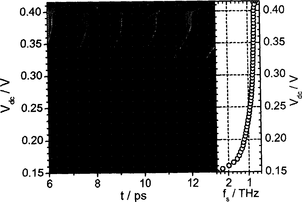
[0018] With the present invention figure 2 The negative effective mass p of the P-type quantum well given in the inset + pp + The device structure of the diode is for the NEM p with p-region length l=0.25μm + pp + Negative effective mass oscillator, if the p-region doping concentration is N a =4.8×10 17 cm -3 , the lattice temperature is T=77K, then when the DC bias V dc When changing from 0.415V to 0.15V, the self-oscillation frequency f s Rising from 0.6THz to 2.6THz ( image 3 ). The semiconductor described in this embodiment is GaAs or AlGaAs.
Login to View More PUM
| Property | Measurement | Unit |
|---|---|---|
| Length | aaaaa | aaaaa |
Abstract
Present invention provides THz radiative generation method based on semiconductor quantum well negative effective mass system, and P quantum well negative effective mass p + pp + diode device structure. Under appropriate doping and bias condition, diode generates THz electric current self-oscillation due to high-field domain forming, designing tunable semiconductor quantum well negative effective mass THz oscillation source, said oscillation source having compactness, light in weight, easy integrating etc advantages.
Description
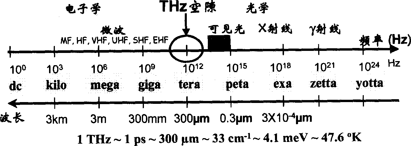
technical field [0001] The invention provides a method for generating THz radiation based on III-V compound semiconductor quantum well materials, and belongs to the technical field of semiconductor optoelectronic materials and devices. Background technique [0002] Terahertz (Terahertz, THz, 1THz=10 12 Hz) frequency band refers to the electromagnetic radiation area with a frequency ranging from a few tenths to a dozen terahertz, which is quite wide between millimeter waves and infrared light (see figure 1 : Electromagnetic Spectrum). It has great application prospects in physics, material science, medical imaging, radio astronomy, military radar, broadband and secure communication, especially inter-satellite communication. For a long time, due to the lack of effective THz generation and detection methods, people's understanding of the nature of electromagnetic radiation in this band is very limited, so that this band is called the "THz gap" in the electromagnetic spectrum,...
Claims
Login to View More Application Information
Patent Timeline
 IPC IPC(8): H01S5/343H01S5/00H01L33/00
Inventor曹俊诚
OwnerSHANGHAI INST OF MICROSYSTEM & INFORMATION TECH CHINESE ACAD OF SCI