Semiconductor quantum well structure capable of modulating microstrip gap by voltage

A voltage modulation, semiconductor technology, applied in the field of semiconductor quantum well structure, can solve the problems affecting the position and size of the microband gap, the quantum well energy level and the wave function effect, etc.

Inactive Publication Date: 2016-10-12
WEST ANHUI UNIV
View PDF4 Cites 2 Cited by
  • Summary
  • Abstract
  • Description
  • Claims
  • Application Information

AI Technical Summary

Problems solved by technology

However, the external electric field can not only adjust the Fermi surface to the microband gap, but also have an important impact on the energy level and wave function of the quantum well, thereby affecting the position and size of its microbandgap

Method used


Image

  • Semiconductor quantum well structure capable of modulating microstrip gap by voltage
  • Semiconductor quantum well structure capable of modulating microstrip gap by voltage
  • Semiconductor quantum well structure capable of modulating microstrip gap by voltage

Examples


Embodiment 1

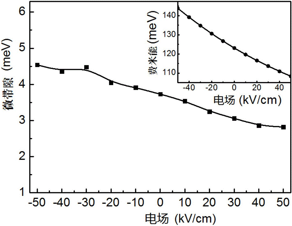
[0016] The thicknesses of the InAs layer and the GaSb layer are 12.5 nm and 10 nm respectively, the thickness of the AlSb layer in the first layer and the fourth layer are both 5 nm, the external electric field is 0 kV / cm, and the ground state energy level of electrons is 45.18 meV, The ground state energy level of holes is 132.04 meV, the Fermi level is 123.07 meV, and the microband gap is 3.73 meV.

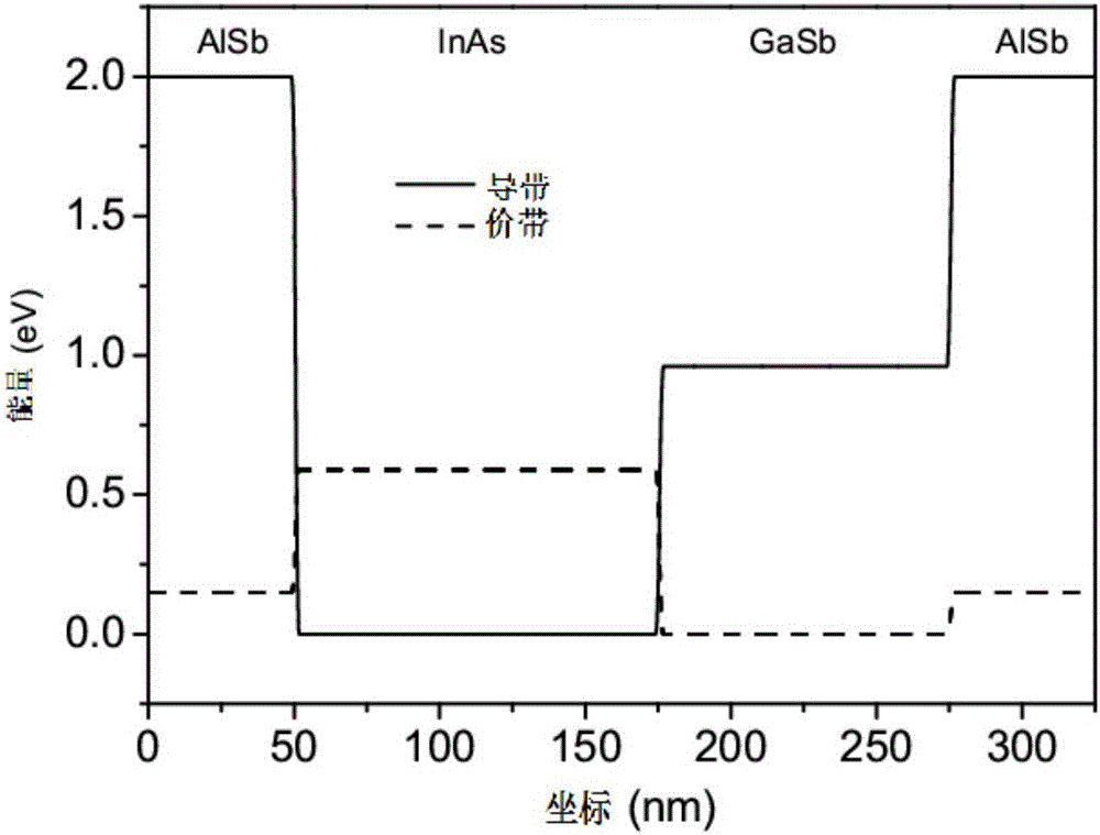
[0017] Please refer to the quantum well structure figure 2 .

Embodiment 2

[0019] The thicknesses of the InAs layer and the GaSb layer are 12.5 nm and 10 nm respectively, the thickness of the AlSb layer in the first layer and the fourth layer are both 5 nm, the external electric field is 50 kV / cm, and the ground state energy level of electrons is 75.03 meV, The ground state energy level of holes is 112.18 meV, the Fermi level is 108.34 meV, and the microband gap is 2.82 meV.

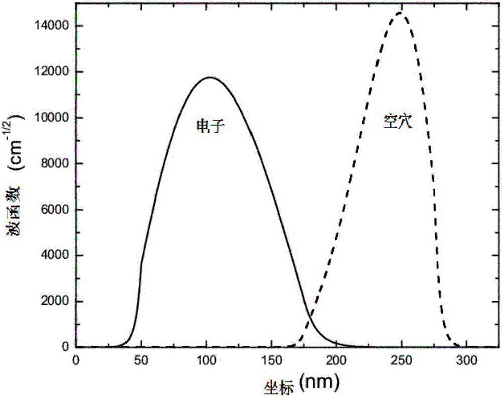
[0020] For the ground state wave functions and hybridization spectra of electrons and holes in this quantum well structure, please refer to image 3 and Figure 4 .

Embodiment 3

[0022] The thicknesses of the InAs layer and the GaSb layer are 12.5 nm and 10 nm respectively, the thickness of the AlSb layer in the first layer and the fourth layer are both 5 nm, the external electric field is -50 kV / cm, and the ground state energy level of electrons is 12.74 meV , the ground state energy level of holes is 158.94meV, the Fermi level is 143.84 meV, and the microband gap is 4.54 meV.


PUM


Abstract

The invention discloses a semiconductor quantum well structure capable of modulating a microstrip gap by voltage. The semiconductor quantum well structure comprises a first quantum well layer, a second quantum well layer, a third quantum well layer, a fourth quantum well layer and additional gate voltage, wherein materials of the first quantum well layer and the second quantum well layer are AlSb; the material of the second quantum well layer is InAs; the material of the third quantum well layer is GaSb; the thicknesses of the first quantum well layer and the fourth quantum well layer are 5-40nm; the thickness of the second quantum well layer is 5-40nm; and the thickness of the third quantum well layer is 5-20nm. Compared with a method for modulating the microstrip gap by changing the thickness of a quantum well, the method for modulating the microstrip gap by the gate voltage disclosed by the invention is more convenient and reliable; and the position of Fermi energy and the size of the microstrip gap can be accurately determined, so that the modulation range of the Fermi energy is further determined. The semiconductor quantum well structure can be widely applied to the aspects of research on the property of a topological insulator of an InAs / GaSb-based semiconductor quantum well system and a device.

Description

technical field [0001] The invention relates to the field of optoelectronic device design, in particular to a semiconductor quantum well structure capable of voltage-modulating micro-bandgap. Background technique [0002] Topological insulator materials are expected to have important applications in devices due to their energy-free nature, which has attracted widespread attention. Topological insulating phases have been observed in graphene, HgTe / CdTe quantum wells, and semiconductor quantum wells based on InAs / GaSb. . Since the HgTe / CdTe quantum well is a true two-dimensional material, it is an ideal choice for studying the properties of topological insulators. However, due to the limitation of the preparation process, it is very difficult to realize the device application. More importantly, in the HgTe / CdTe quantum well, the Fermi surface can only be adjusted by changing the thickness of each layer in the quantum well, so as to observe the topological insulating phase, so...

Claims


Application Information

Patent Timeline
Patent Type & Authority Applications(China)
IPC IPC(8): H01L33/06H01L33/30H01L31/0304H01L31/0352B82Y30/00B82Y40/00
CPCH01L33/06B82Y30/00B82Y40/00H01L31/0304H01L31/035236H01L33/30
Inventor 魏相飞张忠义
Owner WEST ANHUI UNIV
Why Eureka
Try Eureka